FQPF13N50CF Fairchild Semiconductor, FQPF13N50CF Datasheet

MOSFET N-CH 500V 13A TO-220F

FQPF13N50CF

Manufacturer Part Number
FQPF13N50CF
Description
MOSFET N-CH 500V 13A TO-220F
Manufacturer
Fairchild Semiconductor
Series
FRFET™r
Datasheet

Specifications of FQPF13N50CF

Fet Type
MOSFET N-Channel, Metal Oxide
Fet Feature
Standard
Rds On (max) @ Id, Vgs
540 mOhm @ 6.5A, 10V
Drain To Source Voltage (vdss)
500V
Current - Continuous Drain (id) @ 25° C
13A
Vgs(th) (max) @ Id
4V @ 250µA
Gate Charge (qg) @ Vgs
56nC @ 10V
Input Capacitance (ciss) @ Vds
2055pF @ 25V
Power - Max
48W
Mounting Type
Through Hole
Package / Case
TO-220-3 Full Pack (Straight Leads)
Configuration
Single
Transistor Polarity
N-Channel
Resistance Drain-source Rds (on)
0.54 Ohm @ 10 V
Forward Transconductance Gfs (max / Min)
15 S
Drain-source Breakdown Voltage
500 V
Gate-source Breakdown Voltage
+/- 30 V
Continuous Drain Current
13 A
Power Dissipation
48000 mW
Maximum Operating Temperature
+ 150 C
Mounting Style
Through Hole
Minimum Operating Temperature
- 55 C
Lead Free Status / RoHS Status
Lead free / RoHS Compliant

Available stocks

Company
Part Number
Manufacturer
Quantity
Price
Part Number:
FQPF13N50CF
Manufacturer:
FSC
Quantity:
12 000
Part Number:
FQPF13N50CF
Manufacturer:
FAIRCHILD
Quantity:
8 000
Part Number:
FQPF13N50CF
Manufacturer:
FAIRCHILD/仙童
Quantity:
20 000
© 2006 Fairchild Semiconductor Corporation
FQP13N50CF / FQPF13N50CF Rev. A1
F
500V N-Channel MOSFET
Features
• 13A, 500V, R
• Low gate charge (typical 43 nC)
• Low Crss (typical 20pF)
• Fast switching
• 100% avalanche tested
• Improved dv/dt capability
• Fast recovery body diode (typical 100ns)
Absolute Maximum Ratings
*Drain current limited by maximum junction temperature
Thermal Characteristics
V
I
I
V
E
I
E
dv/dt
P
T
T
R
R
Symbol
Symbol
D
DM
AR
J,
L
DSS
GSS
AS
AR
D
θJC
θJA
QP13N50CF / FQPF13N50CF
T
STG
G
Drain-Source Voltage
Drain Current
Drain Current
Gate-Source voltage
Single Pulsed Avalanche Energy
Avalanche Current
Repetitive Avalanche Energy
Peak Diode Recovery dv/dt
Power Dissipation
Maximum Lead Temperature for Soldering Purpose,
1/8” from Case for 5 Seconds
Thermal Resistance, Junction-to-Case
Thermal Resistance, Junction-to-Ambient
Operating and Storage Temperature Range
D
DS(on)
S
= 0.54Ω @V
TO-220
FDP Series
GS
Parameter
- Continuous (T
- Continuous (T
- Pulsed
(T
Parameter
- Derate above 25°C
= 10 V
C
= 25°C)
C
C
= 25°C)
= 100°C)
G
D
S
1
(Note 2)
(Note 1)
(Note 1)
(Note 3)
(Note 1)
Description
These N-Channel enhancement mode power field effect transis-
tors are produced using Fairchild’s proprietary, planar stripe,
DMOS technology.
This advanced technology has been especially tailored to mini-
mize on-state resistance, provide superior switching perfor-
mance, and withstand high energy pulse in the avalanche and
commutation mode. These devices are well suited for high effi-
cient switched mode power supplies and active power factor
correction.
FQP13N50CF FQPF13N50CF
TO-220F
FQPF Series
FQP13N50CF
0.64
62.5
1.56
195
13
52
8
-55 to +150
± 30
19.5
500
530
300
4.5
13
FQPF13N50CF
G
2.58
62.5
FRFET
0.39
13*
52*
48
8*
S
May 2006
D
www.fairchildsemi.com
Unit
°C/W
°C/W
Unit
W/°C
V/ns
mJ
mJ
°C
°C
W
V
A
A
A
V
A
TM

Related parts for FQPF13N50CF

FQPF13N50CF Summary of contents

Page 1

... Thermal Resistance, Junction-to-Case θJC R Thermal Resistance, Junction-to-Ambient θJA © 2006 Fairchild Semiconductor Corporation FQP13N50CF / FQPF13N50CF Rev. A1 Description = 10 V These N-Channel enhancement mode power field effect transis- tors are produced using Fairchild’s proprietary, planar stripe, DMOS technology. This advanced technology has been especially tailored to mini- ...

Page 2

... ≤ 13A, di/dt ≤ 200A/µs, V ≤ Starting DSS, 4. Pulse Test: Pulse width ≤ 300µs, Duty Cycle ≤ Essentially Independent of Operating Temperature Typical Characteristics FQP13N50CF / FQPF13N50CF Rev. A1 Package Reel Size TO-220 - TO-220F - T = 25°C unless otherwise noted C Conditions 250µ ...

Page 3

... I , Drain Current [A] D Figure 5. Capacitance Characteristics 3000 2500 C iss 2000 C oss 1500 1000 C 500 Drain-Source Voltage [V] DS FQP13N50CF / FQPF13N50CF Rev. A1 Figure 2. Transfer Characteristics ※ Notes : 1. 250µs Pulse Test ℃ Figure 4. Body Diode Forward Voltage 10V 20V GS Note : ℃ ...

Page 4

... Single Pulse - Drain-SourceVoltage[V] DS Figure 10. Maximum Drain Current vs. Case Temperature Case Temperature [ ] C FQP13N50CF / FQPF13N50CF Rev. A1 (Continued) Figure 8. On-Resistance Variation 3.0 2.5 2.0 1.5 1.0 Notes : ※ 250 µA 0.5 D 0.0 -100 100 150 200 o C] Figure 9-2. Maximum Safe Operating Area 3 10 ...

Page 5

... Typical Performance Characteristics Figure 11-1. Transient Thermal Response Curve for FQP13N50CF Figure 11-2. Transient Thermal Response Curve for FQPF13N50CF FQP13N50CF / FQPF13N50CF Rev. A1 (Continued) ※ tio tio ( ℃ θ ( θ ※ ( ℃ θ ( θ www.fairchildsemi.com ...

Page 6

... Unclamped Inductive Switching Test Circuit & Waveforms FQP13N50CF / FQPF13N50CF Rev. A1 Gate Charge Test Circuit & Waveform Resistive Switching Test Circuit & Waveforms 6 www.fairchildsemi.com ...

Page 7

... FQP13N50CF / FQPF13N50CF Rev. A1 Peak Diode Recovery dv/dt Test Circuit & Waveforms 7 www.fairchildsemi.com ...

Page 8

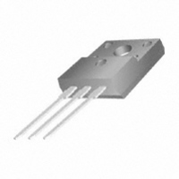
... Mechanical Dimensions 9.90 ø3.60 ±0.10 1.27 2.54TYP ±0.20 [2.54 ] 10.00 FQP13N50CF / FQPF13N50CF Rev. A1 TO-220 ±0.20 (8.70) ±0.10 ±0.10 1.52 ±0.10 0.80 2.54TYP ±0.20 [2.54 ] ±0.20 8 ±0.20 4.50 +0.10 1.30 –0.05 +0.10 ±0.20 0.50 2.40 –0.05 Dimensions in Millimeters www.fairchildsemi.com ...

Page 9

... Mechanical Dimensions MAX1.47 ±0.10 0.80 ±0.10 0.35 2.54TYP ±0.20 [2.54 ] FQP13N50CF / FQPF13N50CF Rev. A1 (Continued) TO-220F ±0.20 ±0.10 10.16 ø3.18 (7.00) (1.00x45°) #1 2.54TYP ±0.20 [2.54 ] ±0.20 9.40 9 ±0.20 2.54 (0.70) +0.10 0.50 ±0.20 2.76 –0.05 Dimensions in Millimeters www.fairchildsemi.com ...

Page 10

... PRODUCT STATUS DEFINITIONS Definition of Terms Datasheet Identification Advance Information Preliminary No Identification Needed Obsolete FQP13N50CF / FQPF13N50CF Rev. A1 ISOPLANAR™ PowerEdge™ LittleFET™ PowerSaver™ MICROCOUPLER™ PowerTrench ® MicroFET™ ...

Related keywords