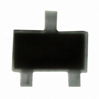
FDY102PZ Fairchild Semiconductor, FDY102PZ Datasheet - Page 3

FDY102PZ
Manufacturer Part Number
FDY102PZ
Description
MOSFET P-CH 20V 830MA SC89-3
Manufacturer
Fairchild Semiconductor
Series
PowerTrench®r
Datasheet
1.FDY102PZ.pdf
(7 pages)
Specifications of FDY102PZ
Fet Type
MOSFET P-Channel, Metal Oxide
Fet Feature
Logic Level Gate
Rds On (max) @ Id, Vgs
500 mOhm @ 830mA, 4.5V
Drain To Source Voltage (vdss)
20V
Current - Continuous Drain (id) @ 25° C
830mA
Vgs(th) (max) @ Id
1V @ 250µA
Gate Charge (qg) @ Vgs
3.1nC @ 4.5V
Input Capacitance (ciss) @ Vds
135pF @ 10V
Power - Max
446mW
Mounting Type
Surface Mount
Package / Case
SC-89-3
Configuration
Single
Transistor Polarity
P-Channel
Resistance Drain-source Rds (on)
0.5 Ohm @ 4.5 V
Drain-source Breakdown Voltage
20 V
Gate-source Breakdown Voltage
+/- 8 V
Continuous Drain Current
0.83 A
Power Dissipation
625 mW
Maximum Operating Temperature
+ 150 C
Mounting Style
SMD/SMT
Minimum Operating Temperature
- 55 C
Lead Free Status / RoHS Status
Lead free / RoHS Compliant
Other names
FDY102PZTR
Available stocks
Company
Part Number
Manufacturer
Quantity
Price
Part Number:
FDY102PZ-NL
Manufacturer:
ON/安森美
Quantity:
20 000
©2010 Fairchild Semiconductor Corporation
FDY102PZ Rev.B2
Typical Characteristics
1.0
0.8
0.6
0.4
0.2
0.0
1.0
0.8
0.6
0.4
0.2
0.0
1.6
1.4
1.2
1.0
0.8
0.6
Figure 3. Normalized On Resistance
Figure 1.
0.0
0.5
-75
Figure 5. Transfer Characteristics
PULSE DURATION = 80
DUTY CYCLE = 0.5% MAX
V
I
V
D
DS
GS
-50
= -0.83 A
vs Junction Temperature
-V
= -5 V
= -4.5 V
DS
T
,
-25
J
On Region Characteristics
DRAIN TO SOURCE VOLTAGE (V)
0.5
-V
,
JUNCTION TEMPERATURE (
GS
V
V
PULSE DURATION = 80
DUTY CYCLE = 0.5% MAX
, GATE TO SOURCE VOLTAGE (V)
T
V
V
1.0
GS
GS
J
GS
GS
0
= 125
= -2.0 V
= -1.8 V
= -4.5 V
= -2.5 V
25
o
P
1.0
C
s
T
J
50
T
= -55
J
= 25 °C unless otherwise noted
T
1.5
75
J
o
C
= 25
P
1.5
s
o
100 125 150
C )
o
V
C
GS
= -1.5 V
2.0
2.0
3
0.001
0.01
4.5
4.0
3.5
3.0
2.5
2.0
1.5
1.0
0.5
2.0
1.6
1.2
0.8
0.4
0.0
0.1
1
0.0
Figure 2.
1.0
Figure 4.
0.0
Forward Voltage vs Source Current
vs Drain Current and Gate Voltage
Figure 6.
V
GS
V
GS
= -1.5 V
1.5
-V
0.2
= 0 V
SD
0.5
-V
Normalized On-Resistance
, BODY DIODE FORWARD VOLTAGE (V)
On-Resistance vs Gate to
GS
-I
T
Source Voltage
D
J
Source to Drain Diode
2.0
,
,
= 125
GATE TO SOURCE VOLTAGE (V)
DRAIN CURRENT (A)
V
0.4
GS
= -1.8 V
1.0
o
C
2.5
PULSE DURATION = 80
DUTY CYCLE = 0.5%MAX
PULSE DURATION = 80
DUTY CYCLE = 0.5% MAX
I
D
0.6
= -0.415 A
3.0
T
1.5
J
= -55
T
T
V
0.8
J
J
T
V
GS
J
= 125
= 25
GS
3.5
= 25
o
= -2.5 V
C
= -4.5 V
V
o
C
2.0
o
GS
o
www.fairchildsemi.com
C
C
1.0
= -2.0V
4.0
P
P
s
s
2.5
4.5
1.2


