FDS3912 Fairchild Semiconductor, FDS3912 Datasheet
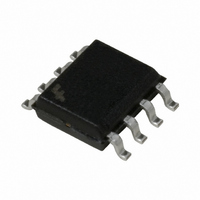
MOSFET N-CH DUAL 100V 3A 8SOIC

FDS3912

Manufacturer Part Number
FDS3912
Description
MOSFET N-CH DUAL 100V 3A 8SOIC
Manufacturer
Fairchild Semiconductor
Series
PowerTrench®r
Datasheet

Specifications of FDS3912

Fet Type
2 N-Channel (Dual)
Fet Feature
Logic Level Gate
Rds On (max) @ Id, Vgs
125 mOhm @ 3A, 10V
Drain To Source Voltage (vdss)
100V
Current - Continuous Drain (id) @ 25° C
3A
Vgs(th) (max) @ Id
4V @ 250µA
Gate Charge (qg) @ Vgs
20nC @ 10V
Input Capacitance (ciss) @ Vds
632pF @ 50V
Power - Max
900mW
Mounting Type
Surface Mount
Package / Case
8-SOIC (3.9mm Width)
Configuration
Dual Dual Drain
Transistor Polarity
N-Channel
Resistance Drain-source Rds (on)
0.125 Ohm @ 10 V
Forward Transconductance Gfs (max / Min)
11 S
Drain-source Breakdown Voltage
100 V
Gate-source Breakdown Voltage
+/- 20 V
Continuous Drain Current
3 A
Power Dissipation
2000 mW
Maximum Operating Temperature
+ 175 C
Mounting Style
SMD/SMT
Minimum Operating Temperature
- 55 C
Lead Free Status / RoHS Status
Lead free / RoHS Compliant

Available stocks

Company
Part Number
Manufacturer
Quantity
Price
Part Number:
FDS3912
Manufacturer:
FSC
Quantity:
10 000
Part Number:
FDS3912
Manufacturer:
FSC
Quantity:
141
Part Number:
FDS3912
Manufacturer:
FAIRCHILD/仙童
Quantity:
20 000
Part Number:
FDS3912-NL
Manufacturer:
FAIRCHILD
Quantity:
12 500
FDS3912
100V Dual N-Channel PowerTrench MOSFET
General Description
These N-Channel MOSFETs have been designed
specifically to improve the overall efficiency of DC/DC
converters using either synchronous or conventional
switching PWM controllers.
These MOSFETs feature faster switching and lower
gate charge than other MOSFETs with comparable
R
easy and safer to drive (even at very high frequencies),
and DC/DC power supply designs with higher overall
efficiency.
2001 Fairchild Semiconductor Corporation
DS(ON)
Absolute Maximum Ratings
Symbol
V
V
I
P
T
Thermal Characteristics
R
R
Package Marking and Ordering Information
D
J
DSS
GSS
D
, T
JA
JC
Device Marking
STG
specifications. The result is a MOSFET that is
FDS3912
Drain-Source Voltage
Gate-Source Voltage
Drain Current
Power Dissipation for Dual Operation
Power Dissipation for Single Operation
Operating and Storage Junction Temperature Range
Thermal Resistance, Junction-to-Ambient
Thermal Resistance, Junction-to-Case
– Continuous
– Pulsed
FDS3912
Device
Parameter
T
A
=25
o
C unless otherwise noted
Reel Size
13’’
(Note 1a)
(Note 1a)
(Note 1b)
(Note 1c)
(Note 1a)
(Note 1)
Features
3 A, 100 V.
Fast switching speed
Low gate charge (14 nC typ)
High performance trench technology for extremely
High power and current handling capability
low R
DS(ON)
5
6
7
8
Tape width
R
R
DS(ON)
DS(ON)
–55 to +175
12mm
Q1
Q2
Ratings
100
1.6
1.0
0.9
20
78
40
20
3
2
= 125 m @ V
= 135 m @ V
October 2001
4
3
2
1
GS
GS
FDS3912 Rev C2(W)
2500 units
Quantity
= 10 V
= 6 V
Units
C/W
C/W
W
V
V
A
C

Related parts for FDS3912

FDS3912 Summary of contents

Page 1

... High power and current handling capability =25 C unless otherwise noted A Ratings (Note 1a) (Note 1a) (Note 1b) (Note 1c) –55 to +175 (Note 1a) (Note 1) Reel Size Tape width 13’’ 12mm October 2001 = 125 135 Units 100 1.6 1.0 0 C/W 40 C/W Quantity 2500 units FDS3912 Rev C2(W) ...

Page 2

... Test Conditions (Note 2) Single Pulse 250 250 A,Referenced – 250 250 A,Referenced 2 125 10V 1.0 MHz GEN Min Typ Max Units 90 mJ 3.0 A 100 V 108 mV 100 nA –100 –6 mV 125 m 98 135 175 250 632 8 4 2.4 nC 3.8 nC FDS3912 Rev C2(W) ...

Page 3

... Pulse Test: Pulse Width < 300 s, Duty Cycle < 2. 1.3 A (Note 100 A/µs (Note determined by the user's board design 125°C/W when mounted 0.02 in pad copper 1.3 A 0.76 1 106 nC c) 135°C/W when mounted on a minimum pad. FDS3912 Rev C2(W) ...

Page 4

... Figure 6. Body Diode Forward Voltage Variation with Source Current and Temperature. = 4.0V GS 4.5V 5.0V 6.0V 10V DRAIN CURRENT ( 1. 125 GATE TO SOURCE VOLTAGE (V) GS Gate-to-Source Voltage 125 -55 C 0.2 0.4 0.6 0 BODY DIODE FORWARD VOLTAGE (V) SD FDS3912 Rev C2( 1.2 ...

Page 5

... Figure 10. Single Pulse Maximum 0.01 0 1MHz ISS C OSS DRAIN TO SOURCE VOLTAGE (V) DS SINGLE PULSE R = 135°C 25°C A 0.01 0 TIME (sec) 1 Power Dissipation. R ( 135 °C/W JA P(pk ( Duty Cycle 100 FDS3912 Rev C2(W) 100 100 2 1000 ...

Page 6

CROSSVOLT â â â â ...

Related keywords