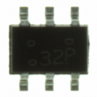
FDG6332C_F085 Fairchild Semiconductor, FDG6332C_F085 Datasheet - Page 5

FDG6332C_F085
Manufacturer Part Number
FDG6332C_F085
Description
MOSFET N/P-CH 20V SC70-6
Manufacturer
Fairchild Semiconductor
Datasheet
1.FDG6332C_F085.pdf
(8 pages)
Specifications of FDG6332C_F085
Fet Type
N and P-Channel
Fet Feature
Logic Level Gate
Rds On (max) @ Id, Vgs
300 mOhm @ 700mA, 4.5V
Drain To Source Voltage (vdss)
20V
Current - Continuous Drain (id) @ 25° C
700mA, 600mA
Vgs(th) (max) @ Id
1.5V @ 250µA
Gate Charge (qg) @ Vgs
1.5nC @ 4.5V
Input Capacitance (ciss) @ Vds
113pF @ 10V
Power - Max
300mW
Mounting Type
Surface Mount
Package / Case
SC-70-6, SC-88, SOT-363
Configuration
Dual
Transistor Polarity
N and P-Channel
Resistance Drain-source Rds (on)
0.3 Ohm @ 4.5 V @ Q1
Drain-source Breakdown Voltage
20 V
Gate-source Breakdown Voltage
+/- 12 V
Continuous Drain Current
0.7 A @ Q1 or 0.6 A @ Q2
Power Dissipation
300 mW
Maximum Operating Temperature
+ 150 C
Mounting Style
SMD/SMT
Minimum Operating Temperature
- 55 C
Lead Free Status / RoHS Status
Lead free / RoHS Compliant
Other names
FDG6332C_F085TR
Available stocks
Company
Part Number
Manufacturer
Quantity
Price
Part Number:
FDG6332C_F085
Manufacturer:
FAIRCHILD/仙童
Quantity:
20 000
Typical Characteristics: N-Channel
0.01
0.1
10
1
5
4
3
2
1
0
0.1
Figure 9. Maximum Safe Operating Area.
0
Figure 7. Gate Charge Characteristics.
SINGLE PULSE
I
R
R
D
DS(ON)
= 0.7A
V
JA
T
GS
A
= 415
= 25
= 4.5V
LIMIT
o
o
C
C/W
0.4
V
DS
, DRAIN-SOURCE VOLTAGE (V)
Q
1
g
, GATE CHARGE (nC)
DC
V
0.8
1s
DS
100ms
= 5V
10ms
10
15V
1ms
100 s
1.2
10V
1.6
100
200
150
100
10
50
8
6
4
2
0
0.001
0
Figure 8. Capacitance Characteristics.
0
C
Figure 10. Single Pulse Maximum
RSS
0.01
C
OSS
V
Power Dissipation.
DS
5
, DRAIN TO SOURCE VOLTAGE (V)
C
ISS
0.1
t
1
, TIME (sec)
10
1
SINGLE PULSE
R
15
JA
FDG6332C_F085 Rev C2 (W)
T
10
A
= 415°C/W
= 25°C
V
f = 1MHz
GS
= 0 V
100
20


