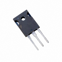
HGTG10N120BND Fairchild Semiconductor, HGTG10N120BND Datasheet - Page 3

HGTG10N120BND
Manufacturer Part Number
HGTG10N120BND
Description
IGBT N-CH NPT 1200V 35A TO-247
Manufacturer
Fairchild Semiconductor
Datasheet
1.HGTG10N120BND.pdf
(8 pages)
Specifications of HGTG10N120BND
Igbt Type
NPT
Voltage - Collector Emitter Breakdown (max)
1200V
Vce(on) (max) @ Vge, Ic
2.7V @ 15V, 10A
Current - Collector (ic) (max)
35A
Power - Max
298W
Input Type
Standard
Mounting Type
Through Hole
Package / Case
TO-247-3
Configuration
Single
Collector- Emitter Voltage Vceo Max
1200 V
Collector-emitter Saturation Voltage
2.45 V
Maximum Gate Emitter Voltage
+/- 20 V
Continuous Collector Current At 25 C
17 A
Gate-emitter Leakage Current
+/- 250 nA
Power Dissipation
298 W
Maximum Operating Temperature
+ 150 C
Continuous Collector Current Ic Max
35 A
Minimum Operating Temperature
- 55 C
Mounting Style
Through Hole
Transistor Type
IGBT
Dc Collector Current
35A
Collector Emitter Voltage Vces
1.2kV
Power Dissipation Pd
298W
Collector Emitter Voltage V(br)ceo
1.2kV
Operating Temperature Range
-55°C To +150°C
Rohs Compliant
Yes
Lead Free Status / RoHS Status
Lead free / RoHS Compliant
Available stocks
Company
Part Number
Manufacturer
Quantity
Price
Company:
Part Number:
HGTG10N120BND
Manufacturer:
MICROCHIP
Quantity:
1 200
©2001 Fairchild Semiconductor Corporation
Electrical Specifications
NOTE:
Typical Performance Curves
Current Turn-On Delay Time
Current Rise Time
Current Turn-Off Delay Time
Current Fall Time
Turn-On Energy
Turn-Off Energy (Note 3)
Diode Forward Voltage
Diode Reverse Recovery Time
Thermal Resistance Junction To Case
3. Turn-Off Energy Loss (E
FIGURE 1. DC COLLECTOR CURRENT vs CASE
at the point where the collector current equals zero (I
of Power Device Turn-Off Switching Loss. This test method produces the true total Turn-Off Energy Loss.
30
25
20
15
10
35
5
0
25
PARAMETER
TEMPERATURE
50
T
C
, CASE TEMPERATURE (
OFF
75
) is defined as the integral of the instantaneous power loss starting at the trailing edge of the input pulse and ending
T
C
= 25
100
o
C, Unless Otherwise Specified (Continued)
Unless Otherwise Specified
o
SYMBOL
C)
t
t
d(OFF)I
d(ON)I
E
R
E
V
OFF
125
t
t
t
θ JC
ON
EC
rr
rI
fI
V
GE
CE
= 15V
= 0A). All devices were tested per JEDEC Standard No. 24-1 Method for Measurement
IGBT and Diode at T
I
V
V
R
L = 2mH
Test Circuit (Figure 20)
I
I
I
IGBT
Diode
150
CE
EC
EC
EC
GE
CE
G
= 10 Ω
= 10A
= 10A
= 10A, dI
= 1A, dI
= 960V
= 15V
TEST CONDITIONS
EC
EC
/dt = 200A/ µ s
/dt = 200A/ µ s
FIGURE 2. MINIMUM SWITCHING SAFE OPERATING AREA
J
60
50
40
30
20
10
0
= 150
0
o
T
C
J
200
V
= 150
CE
, COLLECTOR TO EMITTER VOLTAGE (V)
o
C, R
400
G
= 10Ω, V
MIN
-
-
-
-
-
-
-
-
-
-
-
600
G
= 15V, L = 400µH
TYP
800
1.75
2.55
190
140
1.1
21
11
57
32
-
-
1000
HGTG10N120BND Rev. B
MAX
0.42
1.25
250
200
2.3
1.4
3.2
25
15
70
40
1200
UNITS
o
o
C/W
C/W
mJ
mJ
ns
ns
ns
ns
ns
ns
V
1400


