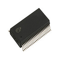
CY8C3665PVI-008 Cypress Semiconductor Corp, CY8C3665PVI-008 Datasheet - Page 8

CY8C3665PVI-008
Manufacturer Part Number
CY8C3665PVI-008
Description
CY8C3665PVI-008
Manufacturer
Cypress Semiconductor Corp
Series
PSOC™ 3 CY8C36xxr
Datasheets
1.CY8C3665LTI-009.pdf
(125 pages)
2.CY8C3665PVI-008.pdf
(108 pages)
3.CY8C3665LTI-044.pdf
(126 pages)
Specifications of CY8C3665PVI-008
Core Processor
8051
Core Size
8-Bit
Speed
67MHz
Connectivity
EBI/EMI, I²C, LIN, SPI, UART/USART
Peripherals
CapSense, DMA, POR, PWM, WDT
Number Of I /o
25
Program Memory Size
32KB (32K x 8)
Program Memory Type
FLASH
Eeprom Size
1K x 8
Ram Size
4K x 8
Voltage - Supply (vcc/vdd)
1.71 V ~ 5.5 V
Data Converters
A/D 2x12b, D/A 4x8b
Oscillator Type
Internal
Operating Temperature
-40°C ~ 85°C
Package / Case
*
Operating Temperature (min)
-40C
Operating Temperature (max)
85C
Technology
CMOS
Processing Unit
Microcontroller
Operating Supply Voltage (min)
1.8V
Operating Supply Voltage (typ)
2.5/3.3/5V
Operating Supply Voltage (max)
5.5V
Package Type
SSOP
Screening Level
Industrial
Pin Count
48
Mounting
Surface Mount
Rad Hardened
No
Processor Series
CY8C36
Core
8051
Data Bus Width
32 bit
Data Ram Size
8 KB
Interface Type
I2C, SPI, UART, USB
Maximum Clock Frequency
67 MHz
Number Of Programmable I/os
28 to 72
Number Of Timers
4
Operating Supply Voltage
0.5 V to 5.5 V
Maximum Operating Temperature
+ 85 C
Mounting Style
SMD/SMT
Controller Family/series
(8051) PSOC 3
No. Of I/o's
25
Eeprom Memory Size
1KB
Ram Memory Size
4KB
Cpu Speed
67MHz
Rohs Compliant
Yes
Lead Free Status / RoHS Status
Lead free / RoHS Compliant
Lead Free Status / RoHS Status
Lead free / RoHS Compliant
Figure 2-5
analog performance on a two-layer board.
For information on circuit board layout issues for mixed signals, refer to the application note
Layout Considerations for PSoC® 3 and PSoC 5.
Notes
Document Number: 001-53413 Rev. *K
11. Pins are Do Not Use (DNU) on devices without USB. The pin must be left floating.
12. This feature on select devices only. See
13. The center pad on the QFN package should be connected to digital ground (Vssd) for best mechanical, thermal, and electrical performance. If not connected to ground,
The two pins labeled Vddd must be connected together.
The two pins labeled Vccd must be connected together, with capacitance added, as shown in
page 28. The trace between the two Vccd pins should be as short as possible.
The two pins labeled Vssd must be connected together.
it should be electrically floated and not connected to any other signal.
and
Figure 2-6
(configurable XRES, GPIO) P1[2]
(TCK, SWDCK, GPIO) P1[1]
(TMS, SWDIO, GPIO) P1[0]
(TDO, SWV, GPIO) P1[3]
(I2C0: SDA, SIO) P12[5]
(I2C0: SCL, SIO) P12[4]
(nTRST, GPIO) P1[5]
on page 10 show an example schematic and an example PCB layout, for the 100-pin TQFP part, for optimal
(TDI, GPIO) P1[4]
(GPIO) P2[5]
(GPIO) P2[6]
(GPIO) P2[7]
(GPIO) P6[4]
(GPIO) P6[5]
(GPIO) P6[6]
(GPIO) P6[7]
(GPIO) P5[0]
(GPIO) P5[1]
(GPIO) P5[2]
(GPIO) P5[3]
Vboost
XRES
Ordering Information
Vssb
Vssd
Vbat
Ind
10
11
12
13
14
15
16
17
18
19
20
21
22
23
24
25
1
2
3
4
5
6
7
8
9
Lines show Vddio
to I/O supply
association
Figure 2-4. 100-pin TQFP Part Pinout
on page 112 for details.
TQFP
75
74
73
72
71
70
69
68
67
66
65
64
63
62
61
60
59
58
57
56
55
54
53
52
51
PSoC
AN57821 - Mixed Signal Circuit Board
Vddio0
P0[3] (GPIO, OpAmp0-/Extref0)
P0[2] (GPIO, OpAmp0+)
P0[1] (GPIO, OpAmp0out)
P0[0] (GPIO, OpAmp2out)
P4[1] (GPIO)
P4[0] (GPIO)
P12[3] (SIO)
P12[2] (SIO)
Vssd
Vdda
Vssa
Vcca
NC
NC
NC
NC
NC
NC
P15[3] (GPIO, kHz XTAL: Xi)
P15[2] (GPIO, kHz XTAL: Xo)
P12[1] (SIO, I2C1: SDA)
P12[0] (SIO, I2C1: SCL)
P3[7] (GPIO, OpAmp3out)
P3[6] (GPIO, OpAmp1out)
Figure 2-5
®
3: CY8C36 Family
and
Power System
[12]
[12]
Data Sheet
Page 8 of 125
on
[+] Feedback


