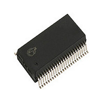
CY8C3665PVI-008 Cypress Semiconductor Corp, CY8C3665PVI-008 Datasheet - Page 21

CY8C3665PVI-008
Manufacturer Part Number
CY8C3665PVI-008
Description
CY8C3665PVI-008
Manufacturer
Cypress Semiconductor Corp
Series
PSOC™ 3 CY8C36xxr
Datasheets
1.CY8C3665LTI-009.pdf
(125 pages)
2.CY8C3665PVI-008.pdf
(108 pages)
3.CY8C3665LTI-044.pdf
(126 pages)
Specifications of CY8C3665PVI-008
Core Processor
8051
Core Size
8-Bit
Speed
67MHz
Connectivity
EBI/EMI, I²C, LIN, SPI, UART/USART
Peripherals
CapSense, DMA, POR, PWM, WDT
Number Of I /o
25
Program Memory Size
32KB (32K x 8)
Program Memory Type
FLASH
Eeprom Size
1K x 8
Ram Size
4K x 8
Voltage - Supply (vcc/vdd)
1.71 V ~ 5.5 V
Data Converters
A/D 2x12b, D/A 4x8b
Oscillator Type
Internal
Operating Temperature
-40°C ~ 85°C
Package / Case
*
Operating Temperature (min)
-40C
Operating Temperature (max)
85C
Technology
CMOS
Processing Unit
Microcontroller
Operating Supply Voltage (min)
1.8V
Operating Supply Voltage (typ)
2.5/3.3/5V
Operating Supply Voltage (max)
5.5V
Package Type
SSOP
Screening Level
Industrial
Pin Count
48
Mounting
Surface Mount
Rad Hardened
No
Processor Series
CY8C36
Core
8051
Data Bus Width
32 bit
Data Ram Size
8 KB
Interface Type
I2C, SPI, UART, USB
Maximum Clock Frequency
67 MHz
Number Of Programmable I/os
28 to 72
Number Of Timers
4
Operating Supply Voltage
0.5 V to 5.5 V
Maximum Operating Temperature
+ 85 C
Mounting Style
SMD/SMT
Controller Family/series
(8051) PSOC 3
No. Of I/o's
25
Eeprom Memory Size
1KB
Ram Memory Size
4KB
Cpu Speed
67MHz
Rohs Compliant
Yes
Lead Free Status / RoHS Status
Lead free / RoHS Compliant
Lead Free Status / RoHS Status
Lead free / RoHS Compliant
5.4 EEPROM
PSoC EEPROM memory is a byte-addressable nonvolatile memory. The CY8C36 has up to 2 KB of EEPROM memory to store user
data. Reads from EEPROM are random access at the byte level. Reads are done directly; writes are done by sending write commands
to an EEPROM programming interface. CPU code execution can continue from flash during EEPROM writes. EEPROM is erasable
and writeable at the row level. The EEPROM is divided into 128 rows of 16 bytes each.
The CPU can not execute out of EEPROM. There is no ECC hardware associated with EEPROM. If ECC is required it must be handled
in firmware.
5.5 Nonvolatile Latches (NVLs)
PSoC has a 4-byte array of nonvolatile latches (NVLs) that are used to configure the device at reset. The NVL register map is shown
in
Table 5-2. Device Configuration NVL Register Map
The details for individual fields and their factory default settings are shown in
Table 5-3. Fields and Factory Default Settings
Although PSoC Creator provides support for modifying the device configuration NVLs, the number of NVL erase / write cycles is limited
– see
Document Number: 001-53413 Rev. *K
PRTxRDM[1:0]
XRESMEN
CFGSPEED
DPS{1:0]
ECCEN
DIG_PHS_DLY[3:0]
Table
Register Address
“Nonvolatile Latches (NVL))”
5-2.
Field
0x00
0x01
0x02
0x03
Controls reset drive mode of the corresponding IO port.
See
are set to the same mode.
Controls whether pin P1[2] is used as a GPIO or as an
external reset. See
description.
Controls the speed of the IMO-based clock during the
device boot process, for faster boot or low-power
operation
Controls the usage of various P1 pins as a debug port.
See
page 59.
Controls whether ECC flash is used for ECC or for general
configuration and data storage. See
Memory”
Selects the digital clock phase delay.
XRESMEN
“Reset Configuration”
“Programming, Debug Interfaces, Resources”
PRT12RDM[1:0]
PRT3RDM[1:0]
7
on page 20.
on page
DIG_PHS_DLY[3:0]
“Pin Descriptions”
100.
6
Description
on page 38. All pins of the port
PRT2RDM[1:0]
PRT6RDM[1:0]
5
“Flash Program
on page 10, XRES
4
on
Table
ECCEN
PRT1RDM[1:0]
PRT5RDM[1:0]
3
00b (default) - high impedance analog
01b - high impedance digital
10b - resistive pull up
11b - resistive pull down
0 (default for 68-pin and 100-pin parts) - GPIO
1 (default for 48-pin parts) - external reset
0 (default) - 12 MHz IMO
1 - 48 MHz IMO
00b - 5-wire JTAG
01b (default) - 4-wire JTAG
10b - SWD
11b - debug ports disabled
0 (default) - ECC disabled
1 - ECC enabled
See the TRM for details.
5-3:.
PSoC
2
DPS[1:0]
®
3: CY8C36 Family
Settings
1
PRT15RDM[1:0]
PRT0RDM[1:0]
PRT4RDM[1:0]
Data Sheet
Page 21 of 125
CFGSPEED
0
[+] Feedback


