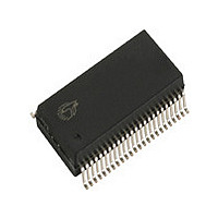
CY8C3665PVI-008 Cypress Semiconductor Corp, CY8C3665PVI-008 Datasheet - Page 78

CY8C3665PVI-008
Manufacturer Part Number
CY8C3665PVI-008
Description
CY8C3665PVI-008
Manufacturer
Cypress Semiconductor Corp
Series
PSOC™ 3 CY8C36xxr
Datasheets
1.CY8C3665LTI-009.pdf
(125 pages)
2.CY8C3665PVI-008.pdf
(108 pages)
3.CY8C3665LTI-044.pdf
(126 pages)
Specifications of CY8C3665PVI-008
Core Processor
8051
Core Size
8-Bit
Speed
67MHz
Connectivity
EBI/EMI, I²C, LIN, SPI, UART/USART
Peripherals
CapSense, DMA, POR, PWM, WDT
Number Of I /o
25
Program Memory Size
32KB (32K x 8)
Program Memory Type
FLASH
Eeprom Size
1K x 8
Ram Size
4K x 8
Voltage - Supply (vcc/vdd)
1.71 V ~ 5.5 V
Data Converters
A/D 2x12b, D/A 4x8b
Oscillator Type
Internal
Operating Temperature
-40°C ~ 85°C
Package / Case
*
Operating Temperature (min)
-40C
Operating Temperature (max)
85C
Technology
CMOS
Processing Unit
Microcontroller
Operating Supply Voltage (min)
1.8V
Operating Supply Voltage (typ)
2.5/3.3/5V
Operating Supply Voltage (max)
5.5V
Package Type
SSOP
Screening Level
Industrial
Pin Count
48
Mounting
Surface Mount
Rad Hardened
No
Processor Series
CY8C36
Core
8051
Data Bus Width
32 bit
Data Ram Size
8 KB
Interface Type
I2C, SPI, UART, USB
Maximum Clock Frequency
67 MHz
Number Of Programmable I/os
28 to 72
Number Of Timers
4
Operating Supply Voltage
0.5 V to 5.5 V
Maximum Operating Temperature
+ 85 C
Mounting Style
SMD/SMT
Controller Family/series
(8051) PSOC 3
No. Of I/o's
25
Eeprom Memory Size
1KB
Ram Memory Size
4KB
Cpu Speed
67MHz
Rohs Compliant
Yes
Lead Free Status / RoHS Status
Lead free / RoHS Compliant
Lead Free Status / RoHS Status
Lead free / RoHS Compliant
11.1.4 XRES
Table 11-16. XRES DC Specifications
Table 11-17. XRES AC Specifications
11.2 Analog Peripherals
Specifications are valid for –40 °C ≤ T
except where noted.
11.2.1 Opamp
Table 11-18. Opamp DC Specifications
Document Number: 001-53413 Rev. *K
V
V
Rpullup
C
V
Idiode
T
V
Vos
TCVos
Ge1
Cin
Vo
Iout
Idd
CMRR
PSRR
Note
Parameter
38.
39. Based on device characterization (Not production tested).
Parameter
Parameter
RESET
IH
IL
H
IOFF
IN
Input offset voltage
Input offset voltage
Input offset voltage drift with temperature
Gain error, unity gain buffer mode
Input capacitance
Output voltage range
Output current, source or sink
Quiescent current
Common mode rejection ratio
Power supply rejection ratio
Input voltage high threshold
Input voltage low threshold
Pull-up resistor
Input capacitance
Input voltage hysteresis
(Schmitt–Trigger)
Current through protection diode to
V
Reset pulse width
DDIO
and V
Description
SSIO
Description
Description
[39]
[39]
A
≤ 85 °C and T
J
Operating temperature –40 °C to
70 °C
Power mode = high
Rload = 1 kΩ
Routing from pin
1 mA, source or sink, power mode =
high
V
–500 mV, V
V
–500 mV, 1.7 V = V
Power mode = min
Power mode = low
Power mode = med
Power mode = high
Vdda
Vdda < 2.7 V
≤ 100 °C, except where noted. Specifications are valid for 1.71 V to 5.5 V,
SSA
SSA
+ 500 mV ≤ Vout ≤ V
+ 500 mV ≤ Vout ≤ V
≥
2.7 V
Conditions
Conditions
Conditions
DDA
> 2.7 V
DDA
≤ 2.7 V
DDA
DDA
PSoC
V
0.7 × V
SSA
Min
Min
Min
3.5
25
16
80
85
70
+ 0.05
–
–
–
–
1
–
–
–
–
–
–
–
–
–
–
DDIO
®
3: CY8C36 Family
1000
Typ
±12
200
250
330
Typ
100
Typ
5.6
–
–
–
–
–
–
–
–
–
–
–
–
–
3
–
–
V
0.05
DDA
Data Sheet
2500
Max
±0.1
V
270
400
950
2.5
18
0.3 ×
Max
Max
100
2
2
–
–
–
–
–
–
8.5
DDIO
Page 78 of 125
–
–
–
–
–
µV / °C
Units
Units
Units
mV
mV
mV
mA
mA
pF
uA
uA
uA
uA
dB
dB
dB
%
mV
V
kΩ
µA
µs
pF
V
V
[+] Feedback


