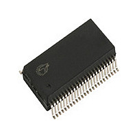
CY8C3665PVI-008 Cypress Semiconductor Corp, CY8C3665PVI-008 Datasheet - Page 58

CY8C3665PVI-008
Manufacturer Part Number
CY8C3665PVI-008
Description
CY8C3665PVI-008
Manufacturer
Cypress Semiconductor Corp
Series
PSOC™ 3 CY8C36xxr
Datasheets
1.CY8C3665LTI-009.pdf
(125 pages)
2.CY8C3665PVI-008.pdf
(108 pages)
3.CY8C3665LTI-044.pdf
(126 pages)
Specifications of CY8C3665PVI-008
Core Processor
8051
Core Size
8-Bit
Speed
67MHz
Connectivity
EBI/EMI, I²C, LIN, SPI, UART/USART
Peripherals
CapSense, DMA, POR, PWM, WDT
Number Of I /o
25
Program Memory Size
32KB (32K x 8)
Program Memory Type
FLASH
Eeprom Size
1K x 8
Ram Size
4K x 8
Voltage - Supply (vcc/vdd)
1.71 V ~ 5.5 V
Data Converters
A/D 2x12b, D/A 4x8b
Oscillator Type
Internal
Operating Temperature
-40°C ~ 85°C
Package / Case
*
Operating Temperature (min)
-40C
Operating Temperature (max)
85C
Technology
CMOS
Processing Unit
Microcontroller
Operating Supply Voltage (min)
1.8V
Operating Supply Voltage (typ)
2.5/3.3/5V
Operating Supply Voltage (max)
5.5V
Package Type
SSOP
Screening Level
Industrial
Pin Count
48
Mounting
Surface Mount
Rad Hardened
No
Processor Series
CY8C36
Core
8051
Data Bus Width
32 bit
Data Ram Size
8 KB
Interface Type
I2C, SPI, UART, USB
Maximum Clock Frequency
67 MHz
Number Of Programmable I/os
28 to 72
Number Of Timers
4
Operating Supply Voltage
0.5 V to 5.5 V
Maximum Operating Temperature
+ 85 C
Mounting Style
SMD/SMT
Controller Family/series
(8051) PSOC 3
No. Of I/o's
25
Eeprom Memory Size
1KB
Ram Memory Size
4KB
Cpu Speed
67MHz
Rohs Compliant
Yes
Lead Free Status / RoHS Status
Lead free / RoHS Compliant
Lead Free Status / RoHS Status
Lead free / RoHS Compliant
8.9.1 Current DAC
The current DAC (IDAC) can be configured for the ranges 0 to
32 µA, 0 to 256 µA, and 0 to 2.048 mA. The IDAC can be
configured to source or sink current.
8.9.2 Voltage DAC
For the voltage DAC (VDAC), the current DAC output is routed
through resistors. The two ranges available for the VDAC are 0
to 1.024 V and 0 to 4.096 V. In voltage mode any load connected
to the output of a DAC should be purely capacitive (the output of
the VDAC is not buffered).
8.10 Up/Down Mixer
In continuous time mode, the SC/CT block components are used
to build an up or down mixer. Any mixing application contains an
input signal frequency and a local oscillator frequency. The
polarity of the clock, Fclk, switches the amplifier between
inverting or noninverting gain. The output is the product of the
input and the switching function from the local oscillator, with
frequency components at the local oscillator plus and minus the
signal frequency (Fclk + Fin and Fclk – Fin) and reduced-level
frequency components at odd integer multiples of the local
oscillator frequency. The local oscillator frequency is provided by
the selected clock source for the mixer.
Continuous time up and down mixing works for applications with
input signals and local oscillator frequencies up to 1 MHz.
Document Number: 001-53413 Rev. *K
Reference
Source
Figure 8-12. DAC Block Diagram
Scaler
Figure 8-13. Mixer Configuration
8.11 Sample and Hold
The main application for a sample and hold, is to hold a value
stable while an ADC is performing a conversion. Some
applications require multiple signals to be sampled
simultaneously, such as for power calculations (V and I).
Figure 8-14. Sample and Hold Topology
(Φ1 and Φ2 are opposite phases of a clock)
V
V
sc_clk
Vin
Vref
n
i
ref
I
R
I
1x , 8x , 64x
1x , 8x , 64x
source
mix
sink
0 20 k or 40 k
Range
Φ
Φ
Range
Φ
Φ
2
2
1
1
3R
R
0
1
PSoC
C
C
1
3
Vout
C2 = 1.7 pF
C1 = 850 fF
®
Φ
Φ
Φ
Φ
R
2
1
2
1
mix
sc_clk
3: CY8C36 Family
0 20 k or 40 k
C
C
Iout
2
4
Data Sheet
Φ
Φ
Φ
Φ
1
2
1
2
Page 58 of 125
V
V
ref
ref
Vout
V
out
[+] Feedback


