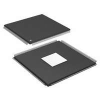
ADSP-21369KSWZ-1A Analog Devices Inc, ADSP-21369KSWZ-1A Datasheet - Page 7

ADSP-21369KSWZ-1A
Manufacturer Part Number
ADSP-21369KSWZ-1A
Description
266 MHz, Shared Memory,S/PDIF EPAD PBfr
Manufacturer
Analog Devices Inc
Series
SHARC®r
Type
Floating Pointr
Datasheet
1.ADSP-21369KBPZ-2A.pdf
(60 pages)
Specifications of ADSP-21369KSWZ-1A
Interface
DAI, DPI
Clock Rate
266MHz
Non-volatile Memory
ROM (768 kB)
On-chip Ram
256kB
Voltage - I/o
3.30V
Voltage - Core
1.20V
Operating Temperature
0°C ~ 70°C
Mounting Type
Surface Mount
Package / Case
208-LQFP
Device Core Size
32/40Bit
Architecture
Super Harvard
Format
Floating Point
Clock Freq (max)
266MHz
Mips
266
Device Input Clock Speed
266MHz
Ram Size
256KB
Program Memory Size
768KB
Operating Supply Voltage (typ)
1.2/3.3V
Operating Supply Voltage (min)
1.14/3.13V
Operating Supply Voltage (max)
1.26/3.47V
Operating Temp Range
0C to 70C
Operating Temperature Classification
Commercial
Mounting
Surface Mount
Pin Count
208
Package Type
LQFP EP
Lead Free Status / RoHS Status
Lead free / RoHS Compliant
For Use With
ADZS-21369-EZLITE - KIT EVAL EZ LITE ADDS-21369
Lead Free Status / Rohs Status
Compliant
Available stocks
Company
Part Number
Manufacturer
Quantity
Price
Company:
Part Number:
ADSP-21369KSWZ-1A
Manufacturer:
Analog Devices Inc
Quantity:
10 000
FAMILY PERIPHERAL ARCHITECTURE
The ADSP-21367/ADSP-21368/ADSP-21369 family contains a
rich set of peripherals that support a wide variety of applications
including high quality audio, medical imaging, communica-
tions, military, test equipment, 3D graphics, speech recognition,
motor control, imaging, and other applications.
External Port
The external port interface supports access to the external mem-
ory through core and DMA accesses. The external memory
address space is divided into four banks. Any bank can be pro-
grammed as either asynchronous or synchronous memory. The
external ports of the ADSP-21367/8/9 processors are comprised
of the following modules.
SDRAM Controller
The SDRAM controller provides an interface of up to four sepa-
rate banks of industry-standard SDRAM devices or DIMMs, at
speeds up to f
each bank has its own memory select line (MS0–MS3), and can
be configured to contain between 16M bytes and 128M bytes of
memory. SDRAM external memory address space is shown in
Table
A set of programmable timing parameters is available to config-
ure the SDRAM banks to support slower memory devices. The
memory banks can be configured as either 32 bits wide for max-
imum performance and bandwidth or 16 bits wide for
minimum device count and lower system cost.
The SDRAM controller address, data, clock, and control pins
can drive loads up to distributed 30 pF loads. For larger memory
systems, the SDRAM controller external buffer timing should
be selected and external buffering should be provided so that the
load on the SDRAM controller pins does not exceed 30 pF.
External Memory
The external port provides a high performance, glueless inter-
face to a wide variety of industry-standard memory devices. The
32-bit wide bus can be used to interface to synchronous and/or
asynchronous memory devices through the use of its separate
internal memory controllers. The first is an SDRAM controller
• An Asynchronous Memory Interface which communicates
• An SDRAM controller that supports a glueless interface
• Arbitration Logic to coordinate core and DMA transfers
• A Shared Memory Interface that allows the connection of
with SRAM, FLASH, and other devices that meet the stan-
dard asynchronous SRAM access protocol. The AMI
supports 14M words of external memory in bank 0 and
16M words of external memory in bank 1, bank 2, and
bank 3.
with any of the standard SDRAMs. The SDC supports 62M
words of external memory in bank 0, and 64M words of
external memory in bank 1, bank 2, and bank 3.
between internal and external memory over the external
port.
up to four ADSP-21368 processors to create shared exter-
nal bus systems (ADSP-21368 only).
4.
SCLK
. Fully compliant with the SDRAM standard,
Rev. E | Page 7 of 60 | July 2009
ADSP-21367/ADSP-21368/ADSP-21369
Table 4. External Memory for SDRAM Addresses
for connection of industry-standard synchronous DRAM
devices and DIMMs (dual inline memory module), while the
second is an asynchronous memory controller intended to
interface to a variety of memory devices. Four memory select
pins enable up to four separate devices to coexist, supporting
any desired combination of synchronous and asynchronous
device types. Non-SDRAM external memory address space is
shown in
Table 5. External Memory for Non-SDRAM Addresses
Shared External Memory
The ADSP-21368 processor supports connecting to common
shared external memory with other ADSP-21368 processors to
create shared external bus processor systems. This support
includes:
Multiple processors can share the external bus with no addi-
tional arbitration logic. Arbitration logic is included on-chip to
allow the connection of up to four processors.
Bus arbitration is accomplished through the BR1–4 signals and
the priority scheme for bus arbitration is determined by the set-
ting of the RPBA pin.
of the pins used in multiprocessor systems.
External Port Throughput
The throughput for the external port, based on 166 MHz clock
and 32-bit data bus, is 221M bytes/s for the AMI and 664M
bytes/s for SDRAM.
Bank
Bank 0
Bank 1
Bank 2
Bank 3
Bank
Bank 0
Bank 1
Bank 2
Bank 3
• Distributed, on-chip arbitration for the shared external bus
• Fixed and rotating priority bus arbitration
• Bus time-out logic
• Bus lock
Table
5.
Size in
Words
62M
64M
64M
64M
Size in
Words
14M
16M
16M
16M
Table 8 on Page 13
Address Range
0x0020 0000–0x00FF FFFF
0x0400 0000–0x04FF FFFF
0x0800 0000–0x08FF FFFF
0x0C00 0000–0x0CFF FFFF
Address Range
0x0020 0000–0x03FF FFFF
0x0400 0000–0x07FF FFFF
0x0800 0000–0x0BFF FFFF
0x0C00 0000–0x0FFF FFFF
provides descriptions


