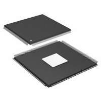
ADSP-21369KSWZ-1A Analog Devices Inc, ADSP-21369KSWZ-1A Datasheet - Page 10

ADSP-21369KSWZ-1A
Manufacturer Part Number
ADSP-21369KSWZ-1A
Description
266 MHz, Shared Memory,S/PDIF EPAD PBfr
Manufacturer
Analog Devices Inc
Series
SHARC®r
Type
Floating Pointr
Datasheet
1.ADSP-21369KBPZ-2A.pdf
(60 pages)
Specifications of ADSP-21369KSWZ-1A
Interface
DAI, DPI
Clock Rate
266MHz
Non-volatile Memory
ROM (768 kB)
On-chip Ram
256kB
Voltage - I/o
3.30V
Voltage - Core
1.20V
Operating Temperature
0°C ~ 70°C
Mounting Type
Surface Mount
Package / Case
208-LQFP
Device Core Size
32/40Bit
Architecture
Super Harvard
Format
Floating Point
Clock Freq (max)
266MHz
Mips
266
Device Input Clock Speed
266MHz
Ram Size
256KB
Program Memory Size
768KB
Operating Supply Voltage (typ)
1.2/3.3V
Operating Supply Voltage (min)
1.14/3.13V
Operating Supply Voltage (max)
1.26/3.47V
Operating Temp Range
0C to 70C
Operating Temperature Classification
Commercial
Mounting
Surface Mount
Pin Count
208
Package Type
LQFP EP
Lead Free Status / RoHS Status
Lead free / RoHS Compliant
For Use With
ADZS-21369-EZLITE - KIT EVAL EZ LITE ADDS-21369
Lead Free Status / Rohs Status
Compliant
Available stocks
Company
Part Number
Manufacturer
Quantity
Price
Company:
Part Number:
ADSP-21369KSWZ-1A
Manufacturer:
Analog Devices Inc
Quantity:
10 000
ADSP-21367/ADSP-21368/ADSP-21369
Peripheral Timers
Three general-purpose timers can generate periodic interrupts
and be independently set to operate in one of three modes:
Each general-purpose timer has one bidirectional pin and four
registers that implement its mode of operation: a 6-bit configu-
ration register, a 32-bit count register, a 32-bit period register,
and a 32-bit pulse width register. A single control and status
register enables or disables all three general-purpose timers
independently.
2-Wire Interface Port (TWI)
The TWI is a bidirectional 2-wire serial bus used to move 8-bit
data while maintaining compliance with the I
The TWI master incorporates the following features:
I/O PROCESSOR FEATURES
The I/O processor provides many channels of DMA, and con-
trols the extensive set of peripherals described in the previous
sections.
DMA Controller
The processor’s on-chip DMA controller allows data transfers
without processor intervention. The DMA controller operates
independently and invisibly to the processor core, allowing
DMA operations to occur while the core is simultaneously exe-
cuting its program instructions. DMA transfers can occur
between the processor’s internal memory and its serial ports, the
SPI-compatible (serial peripheral interface) ports, the IDP
(input data port), the parallel data acquisition port (PDAP), or
the UART.
Thirty four channels of DMA are available on the ADSP-2136x
processors as shown in
Table 6. DMA Channels
Peripheral
SPORTs
PDAP
SPI
UART
External Port
Memory-to-Memory
• Pulse waveform generation mode
• Pulse width count/capture mode
• External event watchdog mode
• Simultaneous master and slave operation on multiple
• Digital filtering and timed event processing
• 7-bit and 10-bit addressing
• 100 kbps and 400 kbps data rates
• Low interrupt rate
device systems with support for multimaster data
arbitration
Table
6.
DMA Channels
16
8
2
4
2
2
2
C bus protocol.
Rev. E | Page 10 of 60 | July 2009
Delay Line DMA
The ADSP-21367/ADSP-21368/ADSP-21369 processors pro-
vide delay line DMA functionality. This allows processor reads
and writes to external delay line buffers (in external memory,
SRAM, or SDRAM) with limited core interaction.
SYSTEM DESIGN
The following sections provide an introduction to system design
options and power supply issues.
Program Booting
The internal memory of the processors can be booted up at sys-
tem power-up from an 8-bit EPROM via the external port, an
SPI master or slave, or an internal boot. Booting is determined
by the boot configuration (BOOT_CFG1–0) pins (see
and the processor hardware reference). Selection of the boot
source is controlled via the SPI as either a master or slave device,
or it can immediately begin executing from ROM.
Table 7. Boot Mode Selection
Power Supplies
The processors have separate power supply connections for the
internal (V
supplies. The internal and analog supplies must meet the 1.3 V
requirement for the 400 MHz device and 1.2 V for the
333 MHz and 266 MHz devices. The external supply must meet
the 3.3 V requirement. All external supply pins must be con-
nected to the same power supply.
Note that the analog supply pin (A
internal clock generator PLL. To produce a stable clock, it is rec-
ommended that PCB designs use an external filter circuit for the
A
A
mended ferrite chip is the muRata BLM18AG102SN1D). To
reduce noise coupling, the PCB should use a parallel pair of
power and ground planes for V
to connect the bypass capacitors to the analog power (A
ground (A
Figure 3
plane on the board—the A
ital ground (GND) at the chip.
BOOT_CFG1–0
00
01
10
11
VDD
VDD
/A
pin. Place the filter components as close as possible to the
VSS
are inputs to the processor and not the analog ground
pins. For an example circuit, see
VSS
DDINT
) pins. Note that the A
), external (V
Booting Mode
SPI Slave Boot
SPI Master Boot
EPROM/FLASH Boot
Reserved
VSS
DDEXT
pin should connect directly to dig-
DDINT
), and analog (A
VDD
VDD
and GND. Use wide traces
) powers the processor’s
and A
Figure
VSS
pins specified in
VDD
3. (A recom-
/A
VSS
Table 7
) power
VDD
) and


