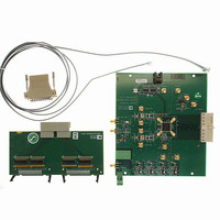
AD9779A-EBZ Analog Devices Inc, AD9779A-EBZ Datasheet - Page 25

AD9779A-EBZ
Manufacturer Part Number
AD9779A-EBZ
Description
Dual 16B, 1.0 GSPS TxDAC
Manufacturer
Analog Devices Inc
Series
TxDAC®r
Datasheet
1.AD9776ABSVZ.pdf
(60 pages)
Specifications of AD9779A-EBZ
Design Resources
Interfacing ADL5370 to AD9779A Dual-Channel, 1 GSPS High Speed DAC (CN0016) Interfacing ADL5371 to AD9779A Dual-Channel, 1 GSPS High Speed DAC (CN0017) Interfacing ADL5372 to AD9779A Dual-Channel, 1 GSPS High Speed DAC (CN0018) Interfacing ADL5373 to AD9779A Dual-Channel, 1 GSPS High Speed DAC (CN0019) Interfacing ADL5374 to AD9779A Dual-Channel, 1 GSPS High Speed DAC (CN0020) Interfacing ADL5375 to AD9779A Dual-Channel, 1 GSPS High Speed DAC (CN0021)
Number Of Dac's
2
Number Of Bits
16
Outputs And Type
2, Differential
Sampling Rate (per Second)
1G
Data Interface
Serial
Dac Type
Current
Voltage Supply Source
Analog and Digital
Operating Temperature
-40°C ~ 85°C
Utilized Ic / Part
AD9779A
Lead Free Status / RoHS Status
Lead free / RoHS Compliant
Settling Time
-
Lead Free Status / RoHS Status
Lead free / RoHS Compliant
SERIAL INTERFACE PORT PIN DESCRIPTIONS
Serial Clock (SCLK)
The serial clock pin synchronizes data to and from the device
as well as running the internal state machines. The maximum
frequency of SCLK is 40 MHz. All data input is registered on
the rising edge of SCLK. All data is driven out on the falling
edge of SCLK.
Chip Select (CSB)
Active low input starts and gates a communication cycle. It
allows more than one device to be used on the same serial
communications lines. The SDO and SDIO pins go to a high
impedance state when this input is high. Chip select should
stay low during the entire communication cycle.
Serial Data I/O (SDIO)
Data is always written into the device on this pin. However, this
pin can be used as a bidirectional data line. The configuration
of this pin is controlled by Register 0x00, Bit 7. The default is
Logic 0, configuring the SDIO pin as unidirectional.
Serial Data Out (SDO)
Data is read from this pin for protocols that use separate lines
for transmitting and receiving data. In the case where the device
operates in a single bidirectional I/O mode, this pin does not
output data and is set to a high impedance state.
MSB/LSB TRANSFERS
The serial port can support both MSB first and LSB first data
formats. This functionality is controlled by Register Bit LSB/MSB
First (Register 0x00, Bit 6). The default is MSB first (LSB/MSB
First = 0).
When LSB/MSB first = 0 (MSB first) the instruction and
data bit must be written from MSB to LSB. Multibyte data
transfers in MSB first format start with an instruction byte
that includes the register address of the most significant data
byte. Subsequent data bytes should follow from high address to
low address. In MSB first mode, the serial port internal byte address
generator decrements for each data byte of the multibyte
communication cycle.
When LSB/MSB First = 1 (LSB first) the instruction and data
bit must be written from LSB to MSB. Multibyte data transfers
in LSB first format start with an instruction byte that includes
the register address of the least significant data byte followed by
multiple data bytes. The serial port internal byte address genera-
tor increments for each byte of the multibyte communication cycle.
Rev. A | Page 25 of 60
The serial port controller data address decrements from the data
address written toward 0x00 for multibyte I/O operations if the
MSB first mode is active. The serial port controller address incre-
ments from the data address written toward 0x1F for multibyte
I/O operations if the LSB first mode is active.
SCLK
SCLK
SCLK
SCLK
SDIO
SDIO
SDIO
SDIO
SDO
SDO
CSB
CSB
CSB
CSB
SDO
R/W N1 N0
Figure 53. Serial Register Interface Timing, MSB First
A0
Figure 54. Serial Register Interface Timing, LSB First
Figure 55. Timing Diagram for SPI Register Write
Figure 56. Timing Diagram for SPI Register Read
INSTRUCTION CYCLE
INSTRUCTION CYCLE
INSTRUCTION BIT 7
A1 A2
t
t
DS
DS
DATA BIT n
AD9776A/AD9778A/AD9779A
A4 A3
A3 A4
t
PWH
t
t
DH
DV
t
A2 A1
N0 N1 R/W D0
SCLK
t
PWL
INSTRUCTION BIT 6
A0 D7 D6
DATA BIT n–1
D0
D7 D6
0
0
DATA TRANSFER CYCLE
DATA TRANSFER CYCLE
D1
D1
N
N
0
0
D5
D5
D2
D2
N
N
0
0
D3
D4
D3
D4
N
0
0
N
D5
D2
D2
D5
N
0
0
N
D1
D6
D1
D6
0
N
N
0
D0
D0
D7
D7
N
0
0
N


