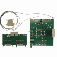
AD9779A-EBZ Analog Devices Inc, AD9779A-EBZ Datasheet - Page 23

AD9779A-EBZ
Manufacturer Part Number
AD9779A-EBZ
Description
Dual 16B, 1.0 GSPS TxDAC
Manufacturer
Analog Devices Inc
Series
TxDAC®r
Datasheet
1.AD9776ABSVZ.pdf
(60 pages)
Specifications of AD9779A-EBZ
Design Resources
Interfacing ADL5370 to AD9779A Dual-Channel, 1 GSPS High Speed DAC (CN0016) Interfacing ADL5371 to AD9779A Dual-Channel, 1 GSPS High Speed DAC (CN0017) Interfacing ADL5372 to AD9779A Dual-Channel, 1 GSPS High Speed DAC (CN0018) Interfacing ADL5373 to AD9779A Dual-Channel, 1 GSPS High Speed DAC (CN0019) Interfacing ADL5374 to AD9779A Dual-Channel, 1 GSPS High Speed DAC (CN0020) Interfacing ADL5375 to AD9779A Dual-Channel, 1 GSPS High Speed DAC (CN0021)
Number Of Dac's
2
Number Of Bits
16
Outputs And Type
2, Differential
Sampling Rate (per Second)
1G
Data Interface
Serial
Dac Type
Current
Voltage Supply Source
Analog and Digital
Operating Temperature
-40°C ~ 85°C
Utilized Ic / Part
AD9779A
Lead Free Status / RoHS Status
Lead free / RoHS Compliant
Settling Time
-
Lead Free Status / RoHS Status
Lead free / RoHS Compliant
THEORY OF OPERATION
The AD9776A/AD9778A/AD9779A have many features that
make them highly suited for wired and wireless communications
systems. The dual digital signal path and dual DAC structure
allow an easy interface with common quadrature modulators
when designing single sideband transmitters. The speed and
performance of the parts allow wider bandwidths and more
carriers to be synthesized than in previously available DACs.
The digital engine uses an innovative filter architecture that
combines the interpolation with a digital quadrature modulator.
This allows the parts to perform digital quadrature frequency
upconversions. The on-chip synchronization circuitry enables
multiple devices to be synchronized to each other, or to a
system clock.
DIFFERENCES BETWEEN AD9776/AD9778/
AD9779 AND AD9776A/AD9778A/AD9779A
REFCLK Maximum Frequency vs. Supply
With some restrictions on the DVDD18 and CVDD18 power
supplies, the AD9776A/AD9778A/AD9779A support a maxi-
mum sample rate of 1100 MHz. Table 2 lists the valid operating
frequencies vs. power supply voltage.
REFCLK Amplitude
With a differential sinusoidal clock applied to REFCLK, the
PLL on the AD9776/AD9778/AD9779 does not achieve optimal
noise performance unless the REFCLK differential amplitude is
increased to 2 V p-p. Note that if an LVPECL driver is used on the
AD9776/AD9778/AD9779, the PLL gives optimal performance if
the REFCLK amplitude is well within LVPECL specifications
(<1.6 V p-p differential). The design of the PLL on the AD9779A
has been improved so that even with a sinusoidal clock, the PLL
still achieves optimal amplitude with the swing = 1.6 V p-p.
PLL Lock Ranges
The individual lock ranges for the AD9776A/AD9778A/AD9779A
PLL are wider than those for the AD9776/AD9778/AD9779.
Table 10.
Part No.
AD9776/AD9778/AD9779
AD9776A/AD9778A/AD9779A
BW Adjustment,
Register 0x0A
Bits<4:0>
11111
01111
Rev. A | Page 23 of 60
PLL Bias Setting,
Register 0x09
Bits<2:0>
111
011
This means that the AD9776A/AD9778A/AD9779A PLL
remains in lock in a given range over a wider temperature range
than the AD9776/ AD9778/AD9779. See Table 21 for PLL lock
ranges for the AD9776A/AD9778A/AD9779A.
PLL Optimal Settings
The optimal settings for the AD9776/AD9778/AD9779 differ
from the AD9776A/AD9778A/AD9779A. Refer to the PLL Bias
Settings section for complete details.
Input Data Delay Line, Manual and Automatic
Correction Modes
The AD9776A/AD9778A/AD9779A can be programmed to
sense when the timing margin on the input data falls below
a preset threshold and to take action. The device can be
programmed to either set the IRQ (pin and register) or
automatically reoptimize the timing input data timing.
Input Data Timing
See Table 25 for timing specifications vs. temperature. The
input data timing specifications (setup and hold) have changed
in the AD9776A/AD9778A/AD9779A. They are not the same
as the timing specifications in the AD9776/AD9778/AD9779.
DATACLK Delay Range
In the AD9776/AD9778/AD9779, the input data delay was
controlled by Register 4, Bits<7:4>. At 25°C, the delay was
stepped by approximately 180 ps/increment. In the AD9779A,
an extra bit has been added, which effectively doubles the delay
range. This bit is now located at Register 1, Bit 1. The increment/
step on the AD9776A/AD9778A/AD9779A remains at ~180 ps.
Version Register
The version register (Register 0x1F) of the AD9776A/AD9778A/
AD9779A reads a value of 0x03. The version register of the
AD9776/AD9778/AD9779 reads a value of 0x02.
Optimal PLL Value,
Register 0x0A
Bits<7:5>
010
011
AD9776A/AD9778A/AD9779A
PLL VCO AGC,
Register 0x08
Bits<1:0>
00
11


