AD9779A-EBZ Analog Devices Inc, AD9779A-EBZ Datasheet - Page 24
AD9779A-EBZ
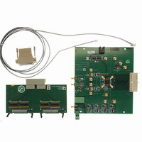
Manufacturer Part Number
AD9779A-EBZ
Description
Dual 16B, 1.0 GSPS TxDAC
Manufacturer
Analog Devices Inc
Series
TxDAC®r
Datasheet
1.AD9776ABSVZ.pdf
(60 pages)
Specifications of AD9779A-EBZ
Design Resources
Interfacing ADL5370 to AD9779A Dual-Channel, 1 GSPS High Speed DAC (CN0016) Interfacing ADL5371 to AD9779A Dual-Channel, 1 GSPS High Speed DAC (CN0017) Interfacing ADL5372 to AD9779A Dual-Channel, 1 GSPS High Speed DAC (CN0018) Interfacing ADL5373 to AD9779A Dual-Channel, 1 GSPS High Speed DAC (CN0019) Interfacing ADL5374 to AD9779A Dual-Channel, 1 GSPS High Speed DAC (CN0020) Interfacing ADL5375 to AD9779A Dual-Channel, 1 GSPS High Speed DAC (CN0021)
Number Of Dac's
2
Number Of Bits
16
Outputs And Type
2, Differential
Sampling Rate (per Second)
1G
Data Interface
Serial
Dac Type
Current
Voltage Supply Source
Analog and Digital
Operating Temperature
-40°C ~ 85°C
Utilized Ic / Part
AD9779A
Lead Free Status / RoHS Status
Lead free / RoHS Compliant
Settling Time
-
Lead Free Status / RoHS Status
Lead free / RoHS Compliant


AD9776A/AD9778A/AD9779A
SERIAL PERIPHERAL INTERFACE
The SPI port is a flexible, synchronous serial communications
port allowing easy interface to many industry-standard micro-
controllers and microprocessors. The port is compatible with
most synchronous transfer formats including both the Motorola
SPI and Intel® SSR protocols.
The interface allows read and write access to all registers
that configure the AD9776A/AD9778A/AD9779A. Single
or multiple byte transfers are supported as well as MSB first
or LSB first transfer formats. Serial data input/output can be
accomplished through a single bidirectional pin (SDIO) or
through two unidirectional pins (SDIO/SDO).
The serial port configuration is controlled by Register 0x00,
Bits<7:6>. It is important to note that any change made to the
serial port configuration occurs immediately upon writing to
the last bit of this byte. Therefore, it is possible with a multibyte
transfer to write to this register and change the configuration in
the middle of a communication cycle. Care must be taken to
compensate for the new configuration within the remaining
bytes of the current communication cycle.
Use of a single byte transfer when changing the serial port
configuration is recommended to prevent unexpected device
behavior.
As described in this section, all serial port data is transferred
to/from the device in synchronization to the SCLK pin. If
synchronization is lost, the device has the ability to asynchro-
nously terminate an I/O operation, putting the serial port
controller into a known state and, thereby, regaining synchro-
nization.
GENERAL OPERATION OF THE SERIAL INTERFACE
There are two phases to a communication cycle with the
AD9776A/AD9778A/AD9779A. Phase 1 is the instruction cycle
(the writing of an instruction byte into the device), coinciding
with the first eight SCLK rising edges. The instruction byte
provides the serial port controller with information regarding
the data transfer cycle, Phase 2 of the communication cycle.
The Phase 1 instruction byte defines whether the upcoming
data transfer is a read or write, the number of bytes in the data
transfer, and the starting register address for the first byte of the
SCLK
SDIO
SDO
CSB
Figure 52. SPI Port
66
67
68
69
PORT
SPI
Rev. A | Page 24 of 60
data transfer. The first eight SCLK rising edges of each commu-
nication cycle are used to write the instruction byte into the device.
A logic high on the CSB pin followed by a logic low resets the
SPI port timing to the initial state of the instruction cycle.
From this state, the next eight rising SCLK edges represent the
instruction bits of the current I/O operation, regardless of the
state of the internal registers or the other signal levels at the
inputs to the SPI port. If the SPI port is in an instruction cycle
or a data transfer cycle, none of the present data is written.
The remaining SCLK edges are for Phase 2 of the communica-
tion cycle. Phase 2 is the actual data transfer between the device
and the system controller. Phase 2 of the communication cycle
is a transfer of one, two, three, or four data bytes as determined
by the instruction byte. Using one multibyte transfer is preferred.
Single byte data transfers are useful in reducing CPU overhead
when register access requires only one byte. Registers change
immediately upon writing to the last bit of each transfer byte.
INSTRUCTION BYTE
See Table 11 for information contained in the instruction byte.
Table 11. SPI Instruction Byte
MSB
I7
R/W
R/ W , Bit 7 of the instruction byte, determines whether a read
or a write data transfer occurs after the instruction byte write.
Logic 1 indicates a read operation. Logic 0 indicates a write
operation.
N1 and N0, Bit 6 and Bit 5 of the instruction byte, determine
the number of bytes to be transferred during the data transfer
cycle. The translation for the number of bytes to be transferred
is listed in Table 12.
A4, A3, A2, A1, and A0—Bit 4, Bit 3, Bit 2, Bit 1, and Bit 0,
respectively—of the instruction byte determine the register that
is accessed during the data transfer portion of the communication
cycle. For multibyte transfers, this address is the starting byte
address. The remaining register addresses are generated by the
device based on the LSB First bit (Register 0x00, Bit 6).
Table 12. Byte Transfer Count
N1
0
0
1
1
I6
N1
N0
0
1
0
1
I5
N0
Description
Transfer one byte
Transfer three bytes
Transfer two bytes
Transfer four bytes
I4
A4
I3
A3
I2
A2
I1
A1
LSB
I0
A0
Related parts for AD9779A-EBZ
Image
Part Number
Description
Manufacturer
Datasheet
Request
R

Part Number:
Description:
Dual 16B, 1.0 GSPS TxDAC
Manufacturer:
Analog Devices Inc
Datasheet:
Part Number:
Description:
BOARD EVALUATION FOR AD9779
Manufacturer:
Analog Devices Inc
Datasheet:
Part Number:
Description:
BOARD EVALUATION FOR AD9779
Manufacturer:
Analog Devices Inc
Datasheet:

Part Number:
Description:
±1.7g Dual-Axis IMEMS Accelerometer Evaluation Board
Manufacturer:
Analog Devices Inc
Datasheet:
Part Number:
Description:
Inertial Sensor Evaluation System
Manufacturer:
Analog Devices Inc
Datasheet:
Part Number:
Description:
Manufacturer:
Analog Devices Inc
Datasheet:
Part Number:
Description:
Manufacturer:
Analog Devices Inc
Datasheet:
Part Number:
Description:
Manufacturer:
Analog Devices Inc
Datasheet:
Part Number:
Description:
Manufacturer:
Analog Devices Inc
Datasheet:
Part Number:
Description:
Manufacturer:
Analog Devices Inc
Datasheet:
Part Number:
Description:
Manufacturer:
Analog Devices Inc
Datasheet:
Part Number:
Description:
Manufacturer:
Analog Devices Inc
Datasheet:
Part Number:
Description:
Manufacturer:
Analog Devices Inc
Datasheet: