AD9779A-EBZ Analog Devices Inc, AD9779A-EBZ Datasheet
AD9779A-EBZ
Specifications of AD9779A-EBZ


Related parts for AD9779A-EBZ


AD9779A-EBZ Summary of contents
Page 1
... Dual 12-/14-/16-Bit,1 GSPS, Digital-to-Analog Converters AD9776A/AD9778A/AD9779A GENERAL DESCRIPTION The AD9776A/AD9778A/AD9779A are dual, 12-/14-/16-bit, high dynamic range, digital-to-analog converters (DACs) that provide a sample rate of 1 GSPS, permitting a multicarrier generation up to the Nyquist frequency. They include features optimized for direct conversion transmit applications, including complex digital modulation, and gain and offset compensation ...
Page 2
... Thermal Resistance ...................................................................... 7 ESD Caution .................................................................................. 7 Pin Configurations and Function Descriptions ........................... 8 Typical Performance Characteristics ........................................... 14 Terminology .................................................................................... 22 Theory of Operation ...................................................................... 23 Differences Between AD9776/AD9778/ AD9779 and AD9776A/AD9778A/AD9779A............................................... 23 Serial Peripheral Interface ............................................................. 24 General Operation of the Serial Interface ............................... 24 Instruction Byte .......................................................................... 24 Serial Interface Port Pin Descriptions ..................................... 25 MSB/LSB Transfers..................................................................... 25 SPI Register Map ............................................................................. 26 Interpolation Filter Architecture ...
Page 3
... FUNCTIONAL BLOCK DIAGRAM CLOCK GENERATION/DISTRIBUTION 2× 2× × /8 DAC ... 7 2× 2× DIGITAL CONTROLLER SERIAL POWER-ON RESET Figure 2. AD9779A Functional Block Diagram Rev Page AD9776A/AD9778A/AD9779A CLOCK REFCLK+ MULTIPLIER 2×/4×/8× REFCLK– SYNC OUT1_P 16-BIT I DAC OUT1_N OUT2_P 16-BIT Q DAC ...
Page 4
... Rev Page mA, maximum sample rate, unless AD9779A Max Min Typ Max Unit 16 Bits ±2.1 LSB ±3.7 LSB +0.001 −0.001 0 +0.001 % FSR ±2 % FSR 31.66 8.66 20 ...
Page 5
... Additional limits on f SYNC_I Register 5, Bits<3:1> in Table 14 SYNC_O SYNC_O− Single-ended DVDD18, CVDD18 = 1.8 V ± 5% DVDD18, CVDD18 = 1.9 V ± 5% DVDD18, CVDD18 = 2.0 V ± 2% Rev Page AD9776A/AD9778A/AD9779A = 20 mA, maximum sample rate, unless OUTFs Min Typ 2.0 300 250 200 112.5 125 137.5 2 ...
Page 6
... Rev Page Unit DACCLK Cycles DACCLK Cycles DACCLK Cycles DACCLK Cycles DACCLK Cycles ms AD9779A Max Min Typ Max Unit 82 dBc 82 dBc 80 dBc 87 dBc 91 dBc 85 dBc 81 dBc 81 dBc −158 dBm/Hz −160 dBm/Hz −161 dBm/Hz 79 dBc 74 dBc ...
Page 7
... V to 100-Lead TQFP_EP DVDD33 + 0.3 V EPAD Soldered −0 CVDD18 + 0.3 V EPAD Not Soldered −0 DVDD33 + 0.3 V ESD CAUTION +125°C −65°C to +150°C Rev Page AD9776A/AD9778A/AD9779A are specified for a 4-layer board in still air θ θ θ 19.1 12.4 7.1 27.4 ...
Page 8
... AD9776A/AD9778A/AD9779A PIN CONFIGURATIONS AND FUNCTION DESCRIPTIONS 100 CVDD18 1 PIN 1 CVDD18 2 CGND 3 CGND 4 REFCLK+ 5 REFCLK– 6 CGND 7 CGND 8 CVDD18 9 CVDD18 10 CGND 11 AGND 12 SYNC_I+ 13 SYNC_I– 14 DGND 15 DVDD18 16 P1D<11> 17 P1D<10> 18 P1D<9> 19 P1D<8> 20 P1D<7> 21 DGND 22 DVDD18 23 P1D<6> 24 P1D<5> CONNECT Table 7. AD9776A Pin Function Descriptions Pin No ...
Page 9
... SPI Port Data Input/Output. 68 SCLK SPI Port Clock. 69 CSB SPI Port Chip Select Bar. 70 RESET Reset, Active High. 71 IRQ Interrupt Request. AD9776A/AD9778A/AD9779A Pin No. Mnemonic Description 72 AGND Analog Ground. 73 IPTAT Factory Test Pin. Output current is proportional to absolute temperature, approximately 14 μA at 25°C with approximately 20 nA/° ...
Page 10
... AD9776A/AD9778A/AD9779A 100 CVDD18 1 PIN 1 CVDD18 2 CGND 3 CGND 4 REFCLK+ 5 REFCLK– 6 CGND 7 CGND 8 CVDD18 9 CVDD18 10 CGND 11 AGND 12 SYNC_I+ 13 SYNC_I– 14 DGND 15 DVDD18 16 P1D<13> 17 P1D<12> 18 P1D<11> 19 P1D<10> 20 P1D<9> 21 DGND 22 DVDD18 23 P1D<8> 24 P1D<7> CONNECT Table 8. AD9778A Pin Function Descriptions Pin No. Mnemonic Description 1 CVDD18 1.8 V Clock Supply. ...
Page 11
... CSB SPI Port Chip Select Bar. 70 RESET Reset, Active High. 71 IRQ Interrupt Request. 72 AGND Analog Ground. AD9776A/AD9778A/AD9779A Pin No. Mnemonic Description 73 IPTAT Factory Test Pin. Output current is proportional to absolute temperature, approximately 14 μA at 25°C with approximately 20 nA/°C slope. This pin should remain floating. ...
Page 12
... DVDD18 16 P1D<15> 17 P1D<14> 18 P1D<13> 19 P1D<12> 20 P1D<11> 21 DGND 22 DVDD18 23 P1D<10> 24 P1D<9> Table 9. AD9779A Pin Function Descriptions Pin No. Mnemonic Description 1 CVDD18 1.8 V Clock Supply. 2 CVDD18 1.8 V Clock Supply. 3 CGND Clock Ground. 4 CGND Clock Ground. 5 REFCLK+ Differential Clock Input. 6 REFCLK− Differential Clock Input. ...
Page 13
... CSB SPI Port Chip Select Bar. 70 RESET Reset, Active High. 71 IRQ Interrupt Request. 72 AGND Analog Ground. AD9776A/AD9778A/AD9779A Pin No. Mnemonic Description 73 IPTAT Factory Test Pin. Output current is proportional to absolute temperature, approximately 14 μA at 25°C with approximately 20 nA/°C slope. This pin should remain floating. ...
Page 14
... OUT Figure 9. AD9779A In-Band SFDR vs. f 2× Interpolation 100 200MSPS = 100MSPS DATA DATA 150MSPS DATA (MHz) OUT Figure 10. AD9779A In-Band SFDR vs. f 4× Interpolation 100 100MSPS = 50MSPS DATA DATA DATA (MHz) OUT Figure 11. AD9779A In-Band SFDR vs. f 8× Interpolation 80 100 ...
Page 15
... OUT Rev Page AD9776A/AD9778A/AD9779A PLL OFF PLL (MHz) OUT f = 100 MSPS, PLL On/Off DATA 0dBFS –3dBFS –6dBFS (MHz) OUT Figure 16. AD9779A In-Band SFDR vs OUT Digital Full Scale 10mA 20mA 30mA (MHz) OUT Figure 17. AD9779A In-Band SFDR vs OUT Output Full-Scale Current ...
Page 16
... OUT Figure 21. AD9779A Third-Order IMD vs. f 8× Interpolation 100 90 80 PLL OFF 70 PLL 100 120 140 f (MHz) OUT Figure 22. AD9779A Third-Order IMD vs. f 4× Interpolation 100 MSPS, PLL On vs. PLL Off DATA 100 120 160 200 240 280 f (MHz) OUT Figure 23 ...
Page 17
... DATA –142 –146 –150 –154 –158 –162 –166 –170 280 320 360 400 Figure 28. AD9779A Noise Spectral Density vs. Digital Full-Scale over Output = 200 MSPS DATA –150 EXT REF –154 DC-COUPLED –158 –162 –166 –170 STOP 400.0MHz Figure 29. AD9779A Noise Spectral Density vs. f Rev ...
Page 18
... OUT Figure 31. AD9779A ACLR for First Adjacent Band W-CDMA, 4× Interpolation 122.88 MSPS, On-Chip Modulation Translates Baseband Signal to IF DATA REF –25.28dBm *ATTEN 4dB *AVG Log 10dB PAVG CENTER 143.88MHz VBW 300kHz *RES BW 30kHz SWEEP 162 ...
Page 19
... Figure 40. AD9778A ACLR, Single Carrier W-CDMA, 4× Interpolation, REF –25.39dBm *AVG Log 10dB PAVG CENTER 143.88MHz *RES BW 30kHz 320 360 400 RMS RESULTS CARRIER POWER –12.74dBm/ 3.84000MHz Figure 41. AD9778A ACLR, f Rev Page AD9776A/AD9778A/AD9779A f = 200MSPS DATA f = 160MSPS DATA f = 250MSPS DATA (MHz) OUT , 2× Interpolation OUT ...
Page 20
... AD9776A/AD9778A/AD9779A –150 –154 f = 200MSPS DAC –158 f DAC –162 f = 800MSPS DAC –166 –170 (MHz) OUT Figure 42. AD9778A Noise Spectral Density vs. f with 500 kHz Spacing 200 MSPS DATA –150 –154 f = 200MSPS DAC f –158 DAC –162 f = 800MSPS DAC –166 –170 (MHz) OUT Figure 43. AD9778A Noise Spectral Density vs − ...
Page 21
... Figure 50. AD9776A Noise Spectral Density vs. f –150 –154 –158 –162 –166 SPAN 50MHz –170 UPPER dBc dBm –75.30 –87.97 –77.99 –90.66 –77.50 –90.17 Rev Page AD9776A/AD9778A/AD9779A f = 200MSPS DAC f = 400MSPS DAC f = 800MSPS DAC (MHz) OUT , Eight-Tone Input ...
Page 22
... AD9776A/AD9778A/AD9779A TERMINOLOGY Integral Nonlinearity (INL) INL is defined as the maximum deviation of the actual analog output from the ideal output, determined by a straight line drawn from zero scale to full scale. Differential Nonlinearity (DNL) DNL is the measure of the variation in analog value, normalized to full scale, associated with a 1 LSB change in digital input code. ...
Page 23
... AD9776/AD9778/AD9779, the PLL gives optimal performance if the REFCLK amplitude is well within LVPECL specifications (<1.6 V p-p differential). The design of the PLL on the AD9779A has been improved so that even with a sinusoidal clock, the PLL still achieves optimal amplitude with the swing = 1.6 V p-p. ...
Page 24
... Figure 52. SPI Port GENERAL OPERATION OF THE SERIAL INTERFACE There are two phases to a communication cycle with the AD9776A/AD9778A/AD9779A. Phase 1 is the instruction cycle (the writing of an instruction byte into the device), coinciding with the first eight SCLK rising edges. The instruction byte provides the serial port controller with information regarding the data transfer cycle, Phase 2 of the communication cycle ...
Page 25
... The serial port internal byte address genera- tor increments for each byte of the multibyte communication cycle. AD9776A/AD9778A/AD9779A The serial port controller data address decrements from the data address written toward 0x00 for multibyte I/O operations if the MSB first mode is active ...
Page 26
... AD9776A/AD9778A/AD9779A SPI REGISTER MAP Note that all unused register bits should be kept at the device default values. Table 13. Address Register Name Hex Decimal Bit 7 Comm 0x00 00 SDIO Bidirectional Digital 0x01 01 Interpolation Factor<1:0> Control 0x02 02 Data Format Sync 0x03 03 DATACLK Control Delay Mode ...
Page 27
... Inverts the polarity of Pin 39, the TXENABLE input pin (also functions as IQSELECT). Q First 0: in interleaved mode, the first byte of a data-word pair is sent to the I DAC 1: in interleaved mode, the first byte of a data-word pair is sent to the Q DAC Rev Page AD9776A/AD9778A/AD9779A Default 0000 ...
Page 28
... AD9776A/AD9778A/AD9779A Register Register Name Address Bits Sync Control 0x03 7 0x03 6 0x03 5:4 0x03 3:0 0x04 7:4 0x04 3:1 0x04 0 0x05 7:4 0x05 3:1 0x05 0 0x06 7:4 0x06 3:0 0x07 7 0x07 6 0x07 5 0x07 4:0 Parameter Function DATACLK Delay Mode 0: manual data timing error correct mode ...
Page 29
... AUX DAC1 off Q DAC Gain Adjustment<9:8> Q DAC 10-bit gain setting word. Bit 9 is the MSB and Bit 0 is the LSB. Q DAC Gain Adjustment<7:0> Q DAC Sleep 0: Q DAC DAC off Q DAC Power-Down 0: Q DAC DAC off Rev Page AD9776A/AD9778A/AD9779A /f . VCO DACCLK / DACCLK / DACCLK /f ...
Page 30
... AD9776A/AD9778A/AD9779A Register Register Name Address Bits AUX DAC2 Control 0x12 1:0 0x11 7:0 0x12 7 0x12 6 0x12 5 Interrupt 0x19 7 0x19 6 0x19 4 0x19 3 0x19 2 0x19 0 Version 0x1F 7:0 Parameter Function Auxiliary DAC2 Data<9:8> AUX DAC2 10-bit output current control word. Magnitude of the AUX DAC current increases with Auxiliary DAC2 Data< ...
Page 31
... INTERPOLATION FILTER ARCHITECTURE The AD9776A/AD9778A/AD9779A can provide up to 8× inter- polation, or the interpolation filters can be entirely disabled important to note that the input signal should be backed off by approximately 0.01 dB from full scale to avoid overflowing the interpolation filters. The coefficients of the low-pass filters and the inverse sinc filter are given in Table 15, Table 16, Table 17, and Table 18 ...
Page 32
... AD9776A/AD9778A/AD9779A 10 0 –10 –20 –30 –40 –50 –60 –70 –80 –90 –100 –4 –3 –2 – (× Input Data Rate) OUT Figure 58. 4× Interpolation, Low-Pass Response to ±4× Input Data Rate (Dotted Lines Indicate 1 dB Roll-Off –10 –20 –30 –40 – ...
Page 33
... The shifted mode capability allows the filter pass band to be placed anywhere in the DAC Nyquist bandwidth. The AD9776A/AD9778A/AD9779A are dual DACs with internal complex modulators built into the interpolating filter response. In dual channel mode, the devices expect the real and ...
Page 34
... AD9776A/AD9778A/AD9779A Table 19. Interpolation Filter Modes, (Register 0x01, Bits<5:2>) Interpolation Factor<7:6> Filter Mode<5:2> 8 0x00 8 0x01 8 0x02 8 0x03 8 0x04 8 0x05 8 0x06 8 0x07 8 0x08 8 0x09 8 0x0A 8 0x0B 8 0x0C 8 0x0D 8 0x0E 8 0x0F 4 0x00 4 0x01 4 0x02 4 0x03 4 0x04 4 0x05 4 0x06 4 0x07 2 0x00 2 0x01 2 0x02 2 0x03 Frequency Normalized to f ...
Page 35
... INTERPOLATION FILTER BANDWIDTH LIMITS The AD9776A/AD9778A/AD9779A use a novel interpolation filter architecture that allows DAC IF frequencies to be gener- ated anywhere in the spectrum. Figure 68 shows the traditional choice of DAC IF output bandwidth placement. Note that there are no possible filter modes in which the carrier can be placed near 0.5 × ...
Page 36
... AD9776A/AD9778A/AD9779A SOURCING THE DAC SAMPLE CLOCK The AD9776A/AD9778A/AD9779A offer two modes of sourcing the DAC sample clock (DACCLK). The first mode employs an on-chip clock multiplier that accepts a reference clock operating at the lower input frequency, most commonly the data input frequency. The on-chip PLL then multiplies the reference clock higher frequency, which can then be used to generate all of the internal clocks required by the DAC ...
Page 37
... If System Startup 1336 Temperature Is 1313 −40°C to −10°C 1299 −10°C to +15°C 1277 15°C to 55°C 1264 55°C to 85°C 1242 1231 Rev Page AD9776A/AD9778A/AD9779A VCO Frequency Range in MHz f f LOW HIGH 1149 1210 1141 1198 1115 1178 1109 1166 ...
Page 38
... AD9776A/AD9778A/AD9779A If the optimal band is in the range (higher VCO frequency), refer to Table 23. Table 23. Setting Optimal PLL Band, When Band Is in the Higher Range (32 to 62) If System Startup Temperature Is Set PLL Band as Follows −40°C to −30°C Set PLL band = readback band + 3 − ...
Page 39
... FS 20 ⎞ ⎞ × ⎟ ⎟ ⎠ ⎠ Rev Page AD9776A/AD9778A/AD9779A AD9776A/AD9778A/AD9779A I DAC GAIN I DAC 1.2V BAND GAP DAC FULL-SCALE CURRENT REFERENCE I120 SCALING CURRENT Q DAC Q DAC GAIN Figure 75. Reference Circuitry 0 200 400 600 800 DAC GAIN CODE Figure 76. I vs. DAC Gain Code ...
Page 40
... LO compensation. AUXILIARY DAC OPERATION Two auxiliary DACs are provided on the AD9776A/AD9778A/ AD9779A. The full-scale output current on these DACs is derived from the 1.2 V band gap reference and external resistor between the I120 pin and ground. The gain scale from the reference ...
Page 41
... QUAD MOD INPUTS 25Ω TO 50Ω –100 Figure 80. AD9779A and ADL5372 with a Multitone Signal at 2.1GHz, No –100 Figure 81. AD9779A and ADL5372 with a Multitone Signal at 2.1 GHz, Gain Rev Page AD9776A/AD9778A/AD9779A RBW 3kHz REF ATT REF LVL VBW ...
Page 42
... INPUT DATA REFERENCED TO DATACLK The simplest method of interfacing to the AD9776A/AD9778A/ AD9779A is when the input data is referenced to the DATACLK output. The DATACLK output is a buffered version (with some fixed delay) of the internal clock that is used to latch the input data. Therefore, if setup and hold times of the input data with respect to DATACLK are met, the input data is latched correctly ...
Page 43
... Rev Page AD9776A/AD9778A/AD9779A t H_SYNC t S_SYNC t SREFCLK t HREFCLK ), but cannot be asserted prior to the previous and the maximum S_SYNC − DACCLK H_SYNC t DACCLK t H_SYNC ...
Page 44
... AD9776A/AD9778A/AD9779A OPTIMIZING THE DATA INPUT TIMING The AD9776A/AD9778A/AD9779A have on-chip circuitry that enables the user to optimize the input data timing by adjusting the relationship between the DATACLK output and DCLK_SMP, the internal clock that samples the input data. This optimization is made by a sequence of SPI register read and write operations. ...
Page 45
... If it has increased, continue incrementing the value of SYNC_I delay until the margin is maximized. If incrementing the SYNC_I delay reduced the timing margin, then the delay should be reduced until the timing margin is optimized. Rev Page AD9776A/AD9778A/AD9779A . DACCLK SYNC_I Rising Edges Required for Synchronization Pulse ...
Page 46
... AD9776A/AD9778A/AD9779A SYNCHRONIZING DEVICES TO A SYSTEM CLOCK The AD9776A/AD9778A/AD9779A offer a pulse mode synchro- nization scheme (see Figure 89) to align the DAC outputs of multiple devices within a system to the same DAC clock edge. The internal clocks are synchronized by providing either a one time pulse or periodic signal to the SYNC_I inputs (SYNC_I+, SYNC_I− ...
Page 47
... INTERPOLATION 1× INTERPOLATION 175 200 225 250 2× INTERPOLATION 1× INTERPOLATION 175 200 225 250 Figure 96. Power Dissipation, Digital 1.8 V Supply, I and Q Data, Dual DAC Rev Page AD9776A/AD9778A/AD9779A ALL INTERPOLATION MODES 100 125 150 175 f (MSPS) DATA Includes Modulation Modes and Zero Stuffing 1.0 8× ...
Page 48
... DAC Figure 99. DVDD18 Power Dissipation of Inverse Sinc Filter POWER-DOWN AND SLEEP MODES The AD9776A/AD9778A/AD9779A have a variety of power- down modes; thus, the digital engine, main TxDACs, or auxiliary DACs can be powered down individually or together. Via the SPI port, the main TxDACs can be placed in sleep or power-down mode. In sleep mode, the TxDAC output is turned off, thus 2× ...
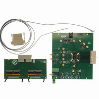
Page 49
... DIGITAL PATTERN GENERATOR CLOCK IN Figure 102. AD9776A/AD9778A/AD9779A Evaluation Board Showing All Connections Figure 101 illustrates the test setup. A sine or square wave clock works well as a clock source. The dc offset on the clock is not a problem, because the clock is ac-coupled on the evaluation board before the REFCLK inputs. All necessary connections to the evaluation board are shown in more detail in Figure 102 ...
Page 50
... AD9776A/AD9778A/AD9779A The evaluation board comes with software that allows the user to program the SPI port. Via the SPI port, the devices can be programmed into any of its various operating modes. When first operating the evaluation board useful to start with a simple configuration, that is, a configuration in which the SPI port settings are as close as possible to the default settings ...
Page 51
... ADL5372 provide an easy-to-interface DAC/modulator combination that can be easily characterized on the evaluation board. Solderable jumpers can be configured to evaluate the single-ended or differential outputs of the AD9776A/AD9778A/ AD9779A. This is the default configuration from the factory and consists of the following jumper positions: • JP2, JP3, JP4, JP8—unsoldered • ...
Page 52
... AD9776A/AD9778A/AD9779A EVALUATION BOARD SCHEMATICS Figure 105. Evaluation Board, Rev. A, Power Supply and Decoupling Rev Page 06452-203 RC0805 RC0805 ...
Page 53
... VDDA 100 ACA 500 500 500 R12 R15 Rev Page AD9776A/AD9778A/AD9779A VOLT E S ACA VOLT E S ACA U1 9779 P2D7 P2D7 50 P2D8 P2D8 49 P2D9 P2D9 48 P2D10 P2D10 47 P2D11 P2D11 46 P2D12 P2D12 45 VSSD_44 44 VDD18_43 43 P2D13 P2D13 42 P2D14 P2D14 41 P2D15 P2D15 33_38 VDDD 38 DCLK ...
Page 54
... AD9776A/AD9778A/AD9779A DNP 0603 RC R24 Figure 107. Evaluation Board, Rev. A, ADL5372 (FMOD2) Quadrature Modulator DNP 21 0603 RC 22 R23 23 24 PAD Rev Page 06452-205 100PF C73 C54 100PF ETC1-1-13 C53 100PF ...
Page 55
... RC0402 RC0402 RC0402 RC0402 CC0402 CC0402 RC0402 Figure 108. Evaluation Board, Rev DAC Clock Interface Rev Page AD9776A/AD9778A/AD9779A 06452-206 ...
Page 56
... AD9776A/AD9778A/AD9779A Figure 109. Evaluation Board, Rev. A, Digital Input Data Lines Rev Page 06452-207 ...
Page 57
... Figure 110. Evaluation Board, Rev. A, On-Board Power Supply Rev Page AD9776A/AD9778A/AD9779A 06452-208 ...
Page 58
... AD9776A/AD9778A/AD9779A Figure 111. Evaluation Board, Rev A, Top Side Silk Screen Rev Page ...
Page 59
... Figure 112. Evaluation Board, Rev. A, Bottom Side Silk Screen Rev Page AD9776A/AD9778A/AD9779A ...
Page 60
... AD9779ABSVZ −40°C to +85°C 1 AD9779ABSVZRL −40°C to +85°C 1 AD9776A-EBZ 1 AD9778A-EBZ 1 AD9779A-EBZ RoHS Compliant Part. ©2007–2008 Analog Devices, Inc. All rights reserved. Trademarks and registered trademarks are the property of their respective owners. 16.00 BSC SQ 14.00 BSC SQ 100 ...