AD9254-150EBZ Analog Devices Inc, AD9254-150EBZ Datasheet - Page 21
AD9254-150EBZ
Manufacturer Part Number
AD9254-150EBZ
Description
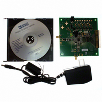
1.8V 14Bit 150 MSPS ADC EB
Manufacturer
Analog Devices Inc
Datasheet
1.AD9254BCPZRL7-150.pdf
(40 pages)
Specifications of AD9254-150EBZ
Number Of Adc's
1
Number Of Bits
14
Sampling Rate (per Second)
150M
Data Interface
Serial
Inputs Per Adc
1 Differential
Input Range
2 Vpp
Power (typ) @ Conditions
506mW @ 150MSPS
Voltage Supply Source
Single Supply
Operating Temperature
-40°C ~ 85°C
Utilized Ic / Part
AD9254
Lead Free Status / RoHS Status
Lead free / RoHS Compliant


SERIAL PORT INTERFACE (SPI)
The AD9254 serial port interface (SPI) allows the user to
configure the converter for specific functions or operations
through a structured register space provided inside the ADC.
This provides the user added flexibility and customization
depending on the application. Addresses are accessed via the
serial port and may be written to or read from via the port.
Memory is organized into bytes that are further divided into
fields, as documented in the Memory Map section. For detailed
operational information, see the
via SPI user
CONFIGURATION USING THE SPI
As summarized in Table 13, three pins define the SPI of this
ADC. The SCLK/DFS pin synchronizes the read and write data
presented to the ADC. The SDIO/DCS dual-purpose pin allows
data to be sent to and read from the internal ADC memory map
registers. The CSB pin is an active low control that enables or
disables the read and write cycles.
Table 13. Serial Port Interface Pins
Pin Name
SCLK/DFS
SDIO/DCS
CSB
The falling edge of the CSB in conjunction with the rising edge
of the SCLK determines the start of the framing. Figure 50 and
Table 14 provide examples of the serial timing and its definitions.
Other modes involving the CSB are available. The CSB can be
held low indefinitely to permanently enable the device (this is
called streaming). The CSB can stall high between bytes to
allow for additional external timing. When CSB is tied high, SPI
functions are placed in a high impedance mode. This mode
turns on any SPI pin secondary functions.
During an instruction phase, a 16-bit instruction is transmitted.
Data follows the instruction phase and the length is determined
by the W0 bit and the W1 bit. All data is composed of 8-bit
words. The first bit of each individual byte of serial data
indicates whether a read or write command is issued. This
allows the serial data input/output (SDIO) pin to change
direction from an input to an output.
manual.
Function
SCLK (serial clock) is the serial shift clock in. SCLK
synchronizes serial interface reads and writes.
SDIO (serial data input/output) is a dual-purpose
pin. The typical role for this pin is an input and
output, depending on the instruction being sent
and the relative position in the timing frame.
CSB (chip select bar) is an active-low control that
gates the read and write cycles.
Interfacing to High Speed ADCs
Rev. 0 | Page 21 of 40
In addition to word length, the instruction phase determines if
the serial frame is a read or write operation, allowing the serial
port to be used to both program the chip as well as read the
contents of the on-chip memory. If the instruction is a readback
operation, performing a readback causes the serial data
input/output (SDIO) pin to change direction from an input to
an output at the appropriate point in the serial frame.
Data can be sent in MSB- or in LSB-first mode. MSB first is the
default on power-up and can be changed via the configuration
register. For more information, see the
ADCs via SPI
Table 14. SPI Timing Diagram Specifications
Name
t
t
t
t
t
t
t
HARDWARE INTERFACE
The pins described in Table 13 comprise the physical interface
between the user’s programming device and the serial port of
the AD9254. The SCLK and CSB pins function as inputs when
using the SPI interface. The SDIO pin is bidirectional, functioning
as an input during write phases and as an output during readback.
The SPI interface is flexible enough to be controlled by either
PROM or PIC microcontrollers. This provides the user with the
ability to use an alternate method to program the ADC. One
method is described in detail in Application Note AN-812,
Microcontroller-Based Serial Port Interface Boot Circuit.
When the SPI interface is not used, some pins serve a dual
function. When strapped to AVDD or ground during device
power on, the pins are associated with a specific function.
CONFIGURATION WITHOUT THE SPI
In applications that do not interface to the SPI control registers,
the SDIO/DCS and SCLK/DFS pins serve as stand-alone
CMOS-compatible control pins. When the device is powered
up, it is assumed that the user intends to use the pins as static
control lines for the output data format and duty cycle stabilizer
(see Table 10). In this mode, the CSB chip select should be
connected to AVDD, which disables the serial port interface.
For more information, see the
via SPI
DS
DH
CLK
S
H
HI
LO
user manual.
Description
Setup time between data and rising edge of SCLK
Hold time between data and rising edge of SCLK
Period of the clock
Setup time between CSB and SCLK
Hold time between CSB and SCLK
Minimum period that SCLK should be in a logic
high state
Minimum period that SCLK should be in a logic
low state
user manual.
Interfacing to High Speed ADCs
Interfacing to High Speed
AD9254
Related parts for AD9254-150EBZ
Image
Part Number
Description
Manufacturer
Datasheet
Request
R

Part Number:
Description:
±1.7g Dual-Axis IMEMS Accelerometer Evaluation Board
Manufacturer:
Analog Devices Inc
Datasheet:

Part Number:
Description:
Inertial Sensor Evaluation System
Manufacturer:
Analog Devices Inc
Datasheet:
Part Number:
Description:
Manufacturer:
Analog Devices Inc
Datasheet:
Part Number:
Description:
Manufacturer:
Analog Devices Inc
Datasheet:
Part Number:
Description:
Manufacturer:
Analog Devices Inc
Datasheet:
Part Number:
Description:
Manufacturer:
Analog Devices Inc
Datasheet:
Part Number:
Description:
Manufacturer:
Analog Devices Inc
Datasheet:
Part Number:
Description:
Manufacturer:
Analog Devices Inc
Datasheet:
Part Number:
Description:
Manufacturer:
Analog Devices Inc
Datasheet:
Part Number:
Description:
Manufacturer:
Analog Devices Inc
Datasheet:
Part Number:
Description:
Manufacturer:
Analog Devices Inc
Datasheet:
Part Number:
Description:
Manufacturer:
Analog Devices Inc
Datasheet:
Part Number:
Description:
Manufacturer:
Analog Devices Inc
Datasheet: