AD9254-150EBZ Analog Devices Inc, AD9254-150EBZ Datasheet - Page 2
AD9254-150EBZ
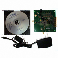
Manufacturer Part Number
AD9254-150EBZ
Description
1.8V 14Bit 150 MSPS ADC EB
Manufacturer
Analog Devices Inc
Datasheet
1.AD9254BCPZRL7-150.pdf
(40 pages)
Specifications of AD9254-150EBZ
Number Of Adc's
1
Number Of Bits
14
Sampling Rate (per Second)
150M
Data Interface
Serial
Inputs Per Adc
1 Differential
Input Range
2 Vpp
Power (typ) @ Conditions
506mW @ 150MSPS
Voltage Supply Source
Single Supply
Operating Temperature
-40°C ~ 85°C
Utilized Ic / Part
AD9254
Lead Free Status / RoHS Status
Lead free / RoHS Compliant


AD9254
TABLE OF CONTENTS
Features .............................................................................................. 1
Applications....................................................................................... 1
General Description ......................................................................... 1
Functional Block Diagram .............................................................. 1
Product Highlights ........................................................................... 1
Revision History ............................................................................... 2
Specifications..................................................................................... 3
Absolute Maximum Ratings............................................................ 7
Pin Configuration and Function Descriptions............................. 8
Equivalent Circuits ........................................................................... 9
Typical Performance Characteristics ........................................... 10
Theory of Operation ...................................................................... 14
REVISION HISTORY
10/06—Revision 0: Initial Version
DC Specifications ......................................................................... 3
AC Specifications.......................................................................... 4
Digital Specifications ................................................................... 5
Switching Specifications .............................................................. 6
Timing Diagram ........................................................................... 6
Thermal Resistance ...................................................................... 7
ESD Caution.................................................................................. 7
Analog Input Considerations.................................................... 14
Differential Input Configurations ............................................ 15
Voltage Reference ....................................................................... 16
Clock Input Considerations ...................................................... 17
Jitter Considerations .................................................................. 19
Power Dissipation and Standby Mode..................................... 19
Digital Outputs ........................................................................... 20
Rev. 0 | Page 2 of 40
Serial Port Interface (SPI).............................................................. 21
Memory Map .................................................................................. 22
Layout Considerations................................................................... 25
Evaluation Board ............................................................................ 26
Outline Dimensions ....................................................................... 40
Timing ......................................................................................... 20
Configuration Using the SPI..................................................... 21
Hardware Interface..................................................................... 21
Configuration Without the SPI ................................................ 21
Reading the Memory Map Register Table............................... 22
Memory Map Register Table..................................................... 23
Power and Ground Recommendations ................................... 25
CML ............................................................................................. 25
RBIAS........................................................................................... 25
Reference Decoupling................................................................ 25
Power Supplies ............................................................................ 26
Input Signals................................................................................ 26
Output Signals ............................................................................ 26
Default Operation and Jumper Selection Settings................. 27
Alternative Clock Configurations............................................ 27
Alternative Analog Input Drive Configuration...................... 27
Schematics................................................................................... 29
Evaluation Board Layout........................................................... 34
Bill of Materials........................................................................... 37
Ordering Guide .......................................................................... 40
Related parts for AD9254-150EBZ
Image
Part Number
Description
Manufacturer
Datasheet
Request
R

Part Number:
Description:
±1.7g Dual-Axis IMEMS Accelerometer Evaluation Board
Manufacturer:
Analog Devices Inc
Datasheet:

Part Number:
Description:
Inertial Sensor Evaluation System
Manufacturer:
Analog Devices Inc
Datasheet:
Part Number:
Description:
Manufacturer:
Analog Devices Inc
Datasheet:
Part Number:
Description:
Manufacturer:
Analog Devices Inc
Datasheet:
Part Number:
Description:
Manufacturer:
Analog Devices Inc
Datasheet:
Part Number:
Description:
Manufacturer:
Analog Devices Inc
Datasheet:
Part Number:
Description:
Manufacturer:
Analog Devices Inc
Datasheet:
Part Number:
Description:
Manufacturer:
Analog Devices Inc
Datasheet:
Part Number:
Description:
Manufacturer:
Analog Devices Inc
Datasheet:
Part Number:
Description:
Manufacturer:
Analog Devices Inc
Datasheet:
Part Number:
Description:
Manufacturer:
Analog Devices Inc
Datasheet:
Part Number:
Description:
Manufacturer:
Analog Devices Inc
Datasheet:
Part Number:
Description:
Manufacturer:
Analog Devices Inc
Datasheet: