AD9254-150EBZ Analog Devices Inc, AD9254-150EBZ Datasheet - Page 15
AD9254-150EBZ
Manufacturer Part Number
AD9254-150EBZ
Description
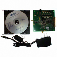
1.8V 14Bit 150 MSPS ADC EB
Manufacturer
Analog Devices Inc
Datasheet
1.AD9254BCPZRL7-150.pdf
(40 pages)
Specifications of AD9254-150EBZ
Number Of Adc's
1
Number Of Bits
14
Sampling Rate (per Second)
150M
Data Interface
Serial
Inputs Per Adc
1 Differential
Input Range
2 Vpp
Power (typ) @ Conditions
506mW @ 150MSPS
Voltage Supply Source
Single Supply
Operating Temperature
-40°C ~ 85°C
Utilized Ic / Part
AD9254
Lead Free Status / RoHS Status
Lead free / RoHS Compliant


DIFFERENTIAL INPUT CONFIGURATIONS
Optimum performance is achieved by driving the AD9254 in a
differential input configuration. For baseband applications, the
AD8138
flexible interface to the ADC. The output common-mode voltage
of the AD8138 is easily set with the CML pin of the AD9254 (see
Figure 32), and the driver can be configured in a Sallen-Key filter
topology to provide band limiting of the input signal.
1V p-p
For baseband applications where SNR is a key parameter,
differential transformer coupling is the recommended input
configuration (see Figure 33). The CML voltage can be
connected to the center tap of the secondary winding of the
transformer to bias the analog input.
The signal characteristics must be considered when selecting
a transformer. Most RF transformers saturate at frequencies
below a few megahertz, and excessive signal power can cause
core saturation, which leads to distortion.
At input frequencies in the second Nyquist zone and above, the
noise performance of most amplifiers is not adequate to achieve
the true SNR performance of the AD9254. For applications
where SNR is a key parameter, transformer coupling is the
recommended input. For applications where SFDR is a key
parameter, differential double balun coupling is the recom-
mended input configuration (see Figure 35).
2V p-p
0.1µF
Figure 32. Differential Input Configuration Using the AD8138
Figure 33. Differential Transformer-Coupled Configuration
differential driver provides excellent performance and a
49.9Ω
49.9Ω
499Ω
523Ω
0.1µF
AD8138
499Ω
499Ω
R
R
R
R
C
C
VIN+
VIN–
VIN+
VIN–
AD9254
AD9254
CML
AVDD
CML
Rev. 0 | Page 15 of 40
As an alternative to using a transformer-coupled input at
frequencies in the second Nyquist zone, the
driver can be used (see Figure 36).
In any configuration, the value of the shunt capacitor, C,
is dependent on the input frequency and source impedance and
may need to be reduced or removed. Table 8 displays recom-
mended values to set the RC network. However, these values are
dependent on the input signal and should only be used as a
starting guide.
Table 8. RC Network Recommended Values
Frequency Range (MHz)
0 to 70
70 to 200
200 to 300
>300
Single-Ended Input Configuration
Although not recommended, it is possible to operate the
AD9254 in a single-ended input configuration, as long as the
input voltage swing is within the AVDD supply. Single-ended
operation can provide adequate performance in cost-sensitive
applications.
In this configuration, SFDR and distortion performance
degrade due to the large input common-mode swing. If the
source impedances on each input are matched, there should be
little effect on SNR performance. Figure 34 details a typical
single-ended input configuration.
1V p-p
10µF
49.9Ω
Figure 34. Single-Ended Input Configuration
0.1µF
10µF
0.1µF
AVDD
1kΩ
1kΩ
1kΩ
1kΩ
AVDD
R Series (Ω) C Differential (pF)
33
33
15
15
R
R
C
15
5
5
Open
AD8352
VIN+
VIN–
AD9254
AD9254
differential
Related parts for AD9254-150EBZ
Image
Part Number
Description
Manufacturer
Datasheet
Request
R

Part Number:
Description:
±1.7g Dual-Axis IMEMS Accelerometer Evaluation Board
Manufacturer:
Analog Devices Inc
Datasheet:

Part Number:
Description:
Inertial Sensor Evaluation System
Manufacturer:
Analog Devices Inc
Datasheet:
Part Number:
Description:
Manufacturer:
Analog Devices Inc
Datasheet:
Part Number:
Description:
Manufacturer:
Analog Devices Inc
Datasheet:
Part Number:
Description:
Manufacturer:
Analog Devices Inc
Datasheet:
Part Number:
Description:
Manufacturer:
Analog Devices Inc
Datasheet:
Part Number:
Description:
Manufacturer:
Analog Devices Inc
Datasheet:
Part Number:
Description:
Manufacturer:
Analog Devices Inc
Datasheet:
Part Number:
Description:
Manufacturer:
Analog Devices Inc
Datasheet:
Part Number:
Description:
Manufacturer:
Analog Devices Inc
Datasheet:
Part Number:
Description:
Manufacturer:
Analog Devices Inc
Datasheet:
Part Number:
Description:
Manufacturer:
Analog Devices Inc
Datasheet:
Part Number:
Description:
Manufacturer:
Analog Devices Inc
Datasheet: