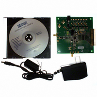
AD9254-150EBZ Analog Devices Inc, AD9254-150EBZ Datasheet - Page 17

AD9254-150EBZ
Manufacturer Part Number
AD9254-150EBZ
Description
1.8V 14Bit 150 MSPS ADC EB
Manufacturer
Analog Devices Inc
Datasheet
1.AD9254BCPZRL7-150.pdf
(40 pages)
Specifications of AD9254-150EBZ
Number Of Adc's
1
Number Of Bits
14
Sampling Rate (per Second)
150M
Data Interface
Serial
Inputs Per Adc
1 Differential
Input Range
2 Vpp
Power (typ) @ Conditions
506mW @ 150MSPS
Voltage Supply Source
Single Supply
Operating Temperature
-40°C ~ 85°C
Utilized Ic / Part
AD9254
Lead Free Status / RoHS Status
Lead free / RoHS Compliant
If the internal reference of the AD9254 is used to drive multiple
converters to improve gain matching, the loading of the reference
by the other converters must be considered. Figure 39 depicts
how the internal reference voltage is affected by loading.
0.1µF
–0.25
–0.50
–0.75
–1.00
–1.25
0.1µF
0
0
Figure 38. Programmable Reference Configuration
0.1µF
Figure 37. Internal Reference Configuration
VREF
0.1µF
SENSE
VREF
VIN+
VIN–
Figure 39. VREF Accuracy vs. Load
SENSE
0.5
R2
R1
VIN+
VIN–
LOAD CURRENT (mA)
SELECT
LOGIC
VREF = 1V
SELECT
LOGIC
1.0
CORE
ADC
AD9254
CORE
0.5V
ADC
AD9254
0.5V
VREF = 0.5V
1.5
REFT
REFB
0.1µF
REFT
REFB
0.1µF
2.0
Rev. 0 | Page 17 of 40
External Reference Operation
The use of an external reference may be necessary to enhance
the gain accuracy of the ADC or improve thermal drift
characteristics. Figure 40 shows the typical drift characteristics
of the internal reference in both 1 V and 0.5 V modes.
When the SENSE pin is tied to AVDD, the internal reference is
disabled, allowing the use of an external reference. An internal
resistor divider loads the external reference with an equivalent
6 kΩ load (see Figure 11). In addition, an internal buffer
generates the positive and negative full-scale references for the
ADC core. Therefore, the external reference must be limited to
a maximum of 1 V.
CLOCK INPUT CONSIDERATIONS
For optimum performance, the AD9254 sample clock inputs
(CLK+ and CLK−) should be clocked with a differential signal.
The signal is typically ac-coupled into the CLK+ pin and the
CLK− pin via a transformer or capacitors. These pins are biased
internally (see Figure 5) and require no external bias.
Clock Input Options
The AD9254 has a very flexible clock input structure. The clock
input can be a CMOS, LVDS, LVPECL, or sine wave signal.
Regardless of the type of signal used, the jitter of the clock
source is of the most concern, as described in the Jitter
Considerations section.
Figure 41 shows one preferred method for clocking the
AD9254. A low jitter clock source is converted from single-
ended to a differential signal using an RF transformer. The
back-to-back Schottky diodes across the transformer secondary
limit clock excursions into the AD9254 to approximately 0.8 V p-p
differential. This helps prevent the large voltage swings of the
clock from feeding through to other portions of the AD9254,
while preserving the fast rise and fall times of the signal, which
are critical to a low jitter performance.
10
8
6
4
2
0
–40
–20
VREF = 0.5V
Figure 40. Typical VREF Drift
0
TEMPERATURE (°C)
VREF = 1V
20
40
60
AD9254
80


