AD9254-150EBZ Analog Devices Inc, AD9254-150EBZ Datasheet
AD9254-150EBZ
Specifications of AD9254-150EBZ


Related parts for AD9254-150EBZ


AD9254-150EBZ Summary of contents
Page 1
... Low cost digital oscilloscopes Macro, micro, and pico cell infrastructure GENERAL DESCRIPTION The AD9254 is a monolithic, single 1.8 V supply, 14-bit, 150 MSPS analog-to-digital converter (ADC), featuring a high performance sample-and-hold amplifier (SHA) and on-chip voltage reference. The product uses a multistage differential pipeline architecture ...
Page 2
... AD9254 TABLE OF CONTENTS Features .............................................................................................. 1 Applications....................................................................................... 1 General Description ......................................................................... 1 Functional Block Diagram .............................................................. 1 Product Highlights ........................................................................... 1 Revision History ............................................................................... 2 Specifications..................................................................................... 3 DC Specifications ......................................................................... 3 AC Specifications.......................................................................... 4 Digital Specifications ................................................................... 5 Switching Specifications .............................................................. 6 Timing Diagram ........................................................................... 6 Absolute Maximum Ratings............................................................ 7 Thermal Resistance ...................................................................... 7 ESD Caution.................................................................................. 7 Pin Configuration and Function Descriptions............................. 8 Equivalent Circuits ........................................................................... 9 Typical Performance Characteristics ........................................... 10 Theory of Operation ...
Page 3
... Full 1.7 2.5 Full 240 Full 11 Full 23 Full 430 Full 450 Full 506 Full 40 Full 1.8 Rev Page AD9254 Unit Max Bits ±0.8 % FSR ±4.5 % FSR LSB ±1.0 LSB LSB ±5.0 LSB ppm/°C ppm/°C ± LSB rms V p-p pF kΩ ...
Page 4
... Full 25°C 25°C 25°C 25°C Full 74 25°C 25°C 25°C 25°C Full 25°C 25°C 25°C 25°C 25°C Rev Page AD9254BCPZ-150 Unit Typ Max 72.0 dBc 71.8 dBc dBc 71.6 dBc 70.8 dBc 71.7 dBc 71.0 dBc dBc 70.6 dBc 69 ...
Page 5
... Full 0 Full −10 +40 Full Full Full = 50 μA) Full 3.29 = 0.5 mA) Full 3.25 Full Full = 50 μA) Full 1.79 = 0.5 mA) Full 1.75 Full Full Rev Page AD9254 AD9254BCPZ-150 Typ Max CMOS/LVDS/LVPECL 1.2 6 AVDD + 1.6 AVDD 3.6 0.8 +10 + 3.6 0.8 −75 + 3.6 0.8 +10 +135 26 2 DRVDD + 0 ...
Page 6
... Full Full Full Full Full CLK – – – – – DCO Figure 2. Timing Diagram Rev Page AD9254BCPZ-150 Min Typ Max 20 150 10 150 6.7 2.0 3.3 4.7 3.0 3.3 3.7 3.1 3.9 4.8 4.4 1.9 2.9 3.0 3.8 12 0.8 0.1 350 3 ...
Page 7
... JA JC Airflow increases heat dissipation, effectively reducing θ addition, metal in direct contact with the package leads from metal traces and through holes, ground, and power planes, reduces the θ ESD CAUTION Rev Page AD9254 θ θ Unit JA JC 26.4 2.4 °C ...
Page 8
... PDWN 38 CLK+ 39 CLK– 43 OEB 44 DCO D2 1 PIN INDICATOR AD9254 D7 6 DRGND 7 TOP VIEW (Not to Scale) DRVDD D10 11 D11 12 Figure 3. Pin Configuration Description Analog Ground. (Pin 0 is the exposed thermal pad on the bottom of the package.) Data Output Bits. Digital Output Ground. ...
Page 9
... SCLK/DFS OEB PDWN Figure 8. Equivalent SCLK/DFS, OEB, PDWN Input Circuit CSB CLK– Figure 9. Equivalent CSB Input Circuit SENSE Figure 10. Equivalent Sense Circuit VREF Figure 11. Equivalent VREF Circuit Rev Page AD9254 1kΩ 30kΩ AVDD 26kΩ 1kΩ 1kΩ AVDD 6kΩ ...
Page 10
... MHz IN 150MSPS 140.3MHz @ –1dBFS SNR = 71.5dBc (72.5dBFS) ENOB = 11.5 BITS SFDR = 81dBc 0 18.75 37.50 56.25 FREQUENCY (MHz) Figure 16. AD9254 Single-Tone FFT with f = 140.3 MHz IN 150MSPS 170.3MHz @ –1dBFS SNR = 70.8dBc (71.8dBFS) ENOB = 11.5 BITS SFDR = 80dBc 0 18.75 37.50 56.25 FREQUENCY (MHz) Figure 17 ...
Page 11
... Figure 22. AD9254 Two-Tone SFDR/IMD3 vs. Input Amplitude (AIN) IN2 90 85 SFDR +25° SFDR +85° SNR +85°C 60 350 and Figure 23. AD9254 Single-Tone SNR/SFDR vs. Input Frequency (f IN Rev Page SFDR (dBFS) SNR (dBFS) SFDR (dBc) 85dBc REFERENCE LINE SNR (dBc) 0 –90 –80 –70 –60 –50 –40 – ...
Page 12
... IN1 95 90 SFDR SNR CLOCK FREQUENCY (MSPS) Figure 25. AD9254 Single-Tone SNR/SFDR vs. Clock Frequency (f with f = 2.4 MHz IN 0 –20 SFDR (–dBc) –40 WORST IMD3 (dBc) –60 –80 SFDR (–dBFS) –100 WORST IMD3 (dBFS) –120 –90 –78 –66 –54 –42 INPUT AMPLITUDE (dBFS) Figure 26 ...
Page 13
... OTUPUT CODE Figure 30. AD9254 DNL with f = 10.3 MHz IN 14336 16384 Rev Page AD9254 ...
Page 14
... REFT be decoupled to REFB by a 0.1 μF capacitor, as described in the Layout Considerations section. Input Common Mode The analog inputs of the AD9254 are not internally dc-biased. In ac-coupled applications, the user must provide this bias externally. Setting the device such that V recommended for optimum performance; however, the device functions over a wider range with reasonable performance (see Figure 30) ...
Page 15
... ADC. The output common-mode voltage of the AD8138 is easily set with the CML pin of the AD9254 (see Figure 32), and the driver can be configured in a Sallen-Key filter topology to provide band limiting of the input signal. ...
Page 16
... Internal Fixed Reference AGND to 0.2 V VOLTAGE REFERENCE A stable and accurate voltage reference is built into the AD9254. The input range is adjustable by varying the reference voltage applied to the AD9254, using either the internal reference or an externally applied reference voltage. The input span of the ADC tracks reference voltage changes linearly ...
Page 17
... R2 SELECT LOGIC SENSE R1 Figure 38. Programmable Reference Configuration If the internal reference of the AD9254 is used to drive multiple converters to improve gain matching, the loading of the reference by the other converters must be considered. Figure 39 depicts how the internal reference voltage is affected by loading. 0 –0.25 VREF = 1V – ...
Page 18
... As a result, these ADCs may be sensitive to clock duty cycle. Commonly, a ±5% tolerance is required on the clock duty cycle to maintain dynamic performance characteristics. The AD9254 contains a duty cycle stabilizer (DCS) that retimes AD9510/ the nonsampling, or falling edge, providing an internal clock family of clock signal with a nominal 50% duty cycle ...
Page 19
... Figure 47. AD9254 Power and Current vs. Clock Frequency f Power-Down Mode By asserting the PDWN pin high, the AD9254 is placed in power- down mode. In this state, the ADC typically dissipates 1.8 mW. During power-down, the output drivers are placed in a high impedance state. Reasserting the PDWN pin low returns the AD9254 to its normal operational mode ...
Page 20
... Digital Output Enable Function (OEB) The AD9254 has three-state ability. If the OEB pin is low, the output data drivers are enabled. If the OEB pin is high, the manual, the data output data drivers are placed in a high impedance state. This is not intended for rapid access to the data bus. Note that OEB is referenced to the digital supplies (DRVDD) and should not exceed that supply voltage ...
Page 21
... The pins described in Table 13 comprise the physical interface between the user’s programming device and the serial port of the AD9254. The SCLK and CSB pins function as inputs when using the SPI interface. The SDIO pin is bidirectional, functioning as an input during write phases and as an output during readback. ...
Page 22
... AD9254 MEMORY MAP READING THE MEMORY MAP REGISTER TABLE Each row in the memory map register table has eight address locations. The memory map is roughly divided into three sections: the chip configuration registers map (Address 0x00 to Address 0x02), the device index and transfer registers map (Address 0xFF), and the ADC functions map (Address 0x08 to Address 0x18) ...
Page 23
... Bit 5 Bit 4 Bit 3 Bit 2 Soft 1 1 Soft reset reset 0 = Off 0 = Off (Default) (Default 8-bit Chip ID Bits 7:0 (AD9254 = 0x00), (default) Open Open Child ID Open 0 = 150 MSPS Open Open Open Open PDWN Open Open Internal power-down mode 000—normal (power-up) 0—Full 001—full power-down 1— ...
Page 24
... AD9254 Addr. Bit 7 (Hex) Parameter Name (MSB) Flexible ADC Functions 10 offset 0D test_io 14 output_mode Output Driver Configuration 00 for DRVDD = 2 3 for DRVDD = 1 output_phase Output Clock Polarity 1 = inverted 0 = normal (Default) 18 VREF Internal Reference Resistor Divider 00—VREF = 1.25 V 01—VREF = 1.5 V 10—VREF = 1.75 V 11— ...
Page 25
... The CML pin should be decoupled to ground with a 0.1 μF capacitor, as shown in Figure 33. RBIAS The AD9254 requires the user to place a 10 kΩ resistor between the RBIAS pin and ground. This resister sets the master current reference of the ADC core and should have at least a 1% tolerance. ...
Page 26
... Figure 53 to Figure 63). Figure 52 shows the typical bench characterization setup used to evaluate the ac performance of the AD9254 critical that the signal sources used for the analog input and clock have very low phase noise (<1 ps rms jitter) to realize the optimum performance of the converter ...
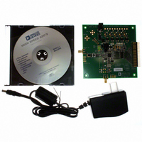
Page 27
... DEFAULT OPERATION AND JUMPER SELECTION SETTINGS The following is a list of the default and optional settings or modes allowed on the AD9254 Rev. A evaluation board. POWER Connect the switching power supply that is supplied in the evaluation kit between a rated 100 240 V ac wall outlet and P500. ...
Page 28
... AD9254 To configure the analog input to drive the AD8352 instead of the default transformer option, the following components need to be added, removed, and/or changed: 1. Remove C1 and C2 in the default analog input path. 2. Populate R3 and R4 with 200 Ω resistors in the analog input path. 3. Populate the optional amplifier input path with all components except R594, R595, and C502 ...
Page 29
... SCHEMATICS RC0402 RC0402 RC040 2 RC040 2 RC0402 CC0402 2 HSMS281 2 HSMS281 RC0402 CC0402 CC0402 RC060 3 RC060 3 Figure 53. Evaluation Board Schematic, DUT Analog Inputs Rev Page AD9254 CC0402 RC060 3 RC060 3 ...
Page 30
... AD9254 Figure 54. Evaluation Board Schematic, DUT, VREF, and Digital Output Interface RC060 3 Rev Page ...
Page 31
... CC0402 CC0402 RC0402 RC060 3 CC0402 CC0402 RC060 3 RC060 3 Figure 55. Evaluation Board Schematic, DUT Clock Input CC0402 CC0402 CC0402 RC0402 RC0402 RC0402 RC0402 S0 S10 GND_PAD S10 VREF 6 RSET RC0402 RC0402 RC0402 RC0402 RC0402 RC0402 Rev Page AD9254 CC0402 ...
Page 32
... AD9254 RC0603 SDO_CHA RC0603 CSB1_CHA RC0603 SDI_CH A RC0603 SCLK_CHA RC0603 RC0603 RC0603 RC0603 RC0603 1 2 PICVCC PICVCC 3 4 GP1 GP1 5 6 GP0 GP0 7 8 MCLR-GP3 MCLR-GP3 RC060 Figure 56. Evaluation Board Schematic, SPI Circuitry Rev Page RC0603 ...
Page 33
... GND GND 1 1 GND GND GND CR500 1 2 Figure 57. Evaluation Board Schematic, Power Supply Inputs Rev Page AD9254 TP509 TP512 TP511 TP510 ...
Page 34
... AD9254 EVALUATION BOARD LAYOUT Figure 58. Evaluation Board Layout, Primary Side Figure 59. Evaluation Board Layout, Secondary Side (Mirrored Image) Rev Page ...
Page 35
... Figure 60. Evaluation Board Layout, Ground Plane Figure 61. Evaluation Board Layout, Power Plane Rev Page AD9254 ...
Page 36
... AD9254 Figure 63. Evaluation Board Layout, Silkscreen Secondary Side (Mirrored Image) Figure 62. Evaluation Board Layout, Silkscreen Primary Side Rev Page ...
Page 37
... Ferrite Bead 3.2 mm × 2.5 mm × 1.6 mm Oscillator SMT 125 MHz or 105 MHz Connector PJ-102A DC power jack Rev Page AD9254 Supplier/Part Number ADI Panasonic LNJ314G8TRA HSMS2812 Micro Commercial Components SK33- TPMSCT-ND Micro Commercial Components S2A- TPMSTR-ND Amber LED Tyco, Raychem ...
Page 38
... AD9254 Omit Item Qty. (DNP) Reference Designator 28 1 P501 29 6 R1, R6, R563, R565, R574, R577 30 5 R2, R5, R561, R562, R571 6 R10, R11, R12, R535, R536, R575 R7, R8, R9, R502, R510, R511 33 6 R500, R501, R576, R578, R579, R581 34 4 R503, R548, R549, R550 ...
Page 39
... Dual buffer IC SC70 Dual buffer IC 48-pin Buffer/line TSSOP driver DUT 48-pin ADC (AD9254) LFCSP_VQ IC 16-pin Differential LFCSP_VQ amplifier Rev Page AD9254 Supplier/Part Number ADI ADP3339AKCZ-1.8 ADI ADP3339AKCZ-2.5 ADI ADP3339AKCZ-3.3 Microchip PIC12F629 Fairchild NC7WZ16 Fairchild NC7WZ07 Fairchild 74VCX162244 ADI AD9254BCPZ ADI AD8352ACPZ ...
Page 40
... Temperature Range 1, 2 AD9254BCPZ-150 –40°C to +85° AD9254BCPZRL7–150 –40°C to +85°C AD9254-150EBZ Pb-free part required that the exposed paddle be soldered to the AGND plane to achieve the best electrical and thermal performance. ©2006 Analog Devices, Inc. All rights reserved. Trademarks and registered trademarks are the property of their respective owners ...