MA160014 Microchip Technology, MA160014 Datasheet - Page 161
MA160014
Manufacturer Part Number
MA160014
Description
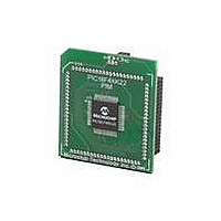
MOD PLUG-IN 44PIN PIC18LF45K22
Manufacturer
Microchip Technology
Series
PIC® XLP™ 18Fr
Datasheet
1.PIC18F26J13-ISS.pdf
(496 pages)
Specifications of MA160014
Accessory Type
Plug-In Module (PIM) - PIC18LF45K10
Product
Microcontroller Modules
Data Bus Width
8 bit
Core Processor
PIC18LF45K22
Interface Type
I2C, SPI
Operating Supply Voltage
1.8 V to 5.5 V
Lead Free Status / RoHS Status
Lead free / RoHS Compliant
For Use With/related Products
PICDEM PIC18 Explorer, DM183032
Lead Free Status / Rohs Status
Lead free / RoHS Compliant
Available stocks
Company
Part Number
Manufacturer
Quantity
Price
Company:

Part Number:
MA160014
Manufacturer:
Microchip Technology
Quantity:
135
Company:
Part Number:
MA160014
Manufacturer:
MICROCHIP
Quantity:
12 000


12.0
The Timer1/3/5 module is a 16-bit timer/counter with
the following features:
• 16-bit timer/counter register pair (TMRxH:TMRxL)
• Programmable internal or external clock source
• 2-bit prescaler
• Dedicated Secondary 32 kHz oscillator circuit
• Optionally synchronized comparator out
• Multiple Timer1/3/5 gate (count enable) sources
• Interrupt on overflow
• Wake-up on overflow (external clock,
• 16-Bit Read/Write Operation
• Time base for the Capture/Compare function
FIGURE 12-1:
2010 Microchip Technology Inc.
Timer2/4/6 Match
Asynchronous mode only)
SYNCC2OUT
PR2/4/6
SYNCC1OUT
Comparator 2
Comparator 1
TxG
TxGSS<1:0>
TIMER1/3/5 MODULE WITH
GATE CONTROL
Note 1:
(7)
(7)
2:
3:
4:
5:
6:
7:
TxCKI
TxGPOL
Set flag bit
TMRxIF on
Overflow
ST Buffer is high speed type when using TxCKI.
Timer1/3/5 register increments on rising edge.
Synchronize does not operate while in Sleep.
See
T1CKI is not available when the secondary oscillator is enabled. (SOSCGO = 1 or TXSOSCEN = 1)
T3CKI is not available when the secondary oscillator is enabled, unless T3CMX = 1.
Synchronized comparator output should not be used in conjunction with synchronized TxCKI.
Secondary
Oscillator
Module
See Figure 2-4
00
10
11
TIMER1/3/5 BLOCK DIAGRAM
01
Figure 12-2
(5)
TxSOSCEN
,(6)
TMRxON
TxGTM
TMRxH
for 16-Bit Read/Write Mode Block Diagram.
SOSCOUT
TMRx
(1)
TxG_IN
(2),(4)
D
R
CK
TMRxL
1
0
Q
Q
TxCLK_EXT_SRC
Preliminary
TMRxCS<1:0>
0
1
Reserved
TxGGO/DONE
Q
Internal
Internal
F
OSC
Clock
Clock
F
OSC
EN
/4
D
• Special Event Trigger (with CCP/ECCP)
• Selectable Gate Source Polarity
• Gate Toggle Mode
• Gate Single-pulse Mode
• Gate Value Status
• Gate Event Interrupt
Figure 12-1
module.
TxCLK
Single Pulse
Acq. Control
11
10
01
00
PIC18(L)F2X/4XK22
TxGSPM
TxCKPS<1:0>
TxSYNC
Prescaler
1, 2, 4, 8
TMRxON
is a block diagram of the Timer1/3/5
0
1
2
0
1
Internal
F
Clock
TxGVAL
OSC
TMRxGE
/2
Q1
Synchronize
Synchronized
Interrupt
clock input
D
EN
det
det
Sleep input
Q
(3),(7)
To Comparator Module
DS41412D-page 161
Set
TMRxGIF
TXGCON
Data Bus
RD
Related parts for MA160014
Image
Part Number
Description
Manufacturer
Datasheet
Request
R

Part Number:
Description:
Manufacturer:
Microchip Technology Inc.
Datasheet:
Part Number:
Description:
Manufacturer:
Microchip Technology Inc.
Datasheet:
Part Number:
Description:
Manufacturer:
Microchip Technology Inc.
Datasheet:
Part Number:
Description:
Manufacturer:
Microchip Technology Inc.
Datasheet:
Part Number:
Description:
Manufacturer:
Microchip Technology Inc.
Datasheet:
Part Number:
Description:
Manufacturer:
Microchip Technology Inc.
Datasheet:
Part Number:
Description:
Manufacturer:
Microchip Technology Inc.
Datasheet:
Part Number:
Description:
Manufacturer:
Microchip Technology Inc.
Datasheet: