CDB42L55 Cirrus Logic Inc, CDB42L55 Datasheet - Page 29
CDB42L55
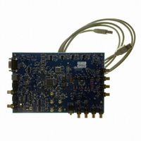
Manufacturer Part Number
CDB42L55
Description
Eval Bd Ultra Low Power Stereo Codec
Manufacturer
Cirrus Logic Inc
Specifications of CDB42L55
Main Purpose
Audio, CODEC
Embedded
Yes, FPGA / CPLD
Utilized Ic / Part
CS42L55
Primary Attributes
2 Stereo Analog Inputs, Stereo Line and Headphone Outputs, S/PDIF Transmitter and Receiver
Secondary Attributes
GUI, USB, RS232, I2C Interfaces, USB or External or Battery Power Supply
Product
Audio Modules
Lead Free Status / RoHS Status
Contains lead / RoHS non-compliant
Lead Free Status / RoHS Status
Contains lead / RoHS non-compliant
Other names
598-1506
CDB-42L55
CDB-42L55


DS773F1
4.5.2
4.5.1.3
When the Adaptive Power bits are set to 11, the CS42L55 decides which of the two sets of rail voltages
to send to the amplifiers based solely upon the level of the signal being sent to the amplifiers. If the signal
that is sent to the amplifiers would cause the amplifiers to clip when operating on the lower set of rail volt-
ages, the control logic instructs the charge pump to provide the higher set of rail voltages (±VCP) to the
amplifiers. If the signal that is sent to the amplifiers would not cause the amplifiers to clip when operating
on the lower set of rail voltages, the control logic instructs the charge pump to provide the lower set of rail
voltages (±VCP/2) to the amplifiers. This mode of operation eliminates the need to advise the CS42L55
of volume settings external to the device.
Note:
alog passthrough (PGA to HP/Line).
Power Supply Transitions
Charge pump transitions from the lower set of rail voltages to the higher set of rail voltages occur on the
next FLYN/P clock cycle. Despite the fast response time of the system, the capacitive elements on the
VHPFILT pins prevent the rail voltages from changing instantaneously. Instead, the rail voltages ramp up
from ±VCP/2 to ±VCP based on the time constant created by the output impedance of the charge pump
and the capacitor on the VHPFILT pin (the transition time is approximately 20 µs). This behavior is de-
tailed in
outputs before the rail voltages charge to the full ±VCP level. This transitory clipping has been found to
be inaudible in listening tests.
Referenced Control
HPxVOL[7:0] .......................
LINExVOL[7:0] ....................
MSTxVOL[7:0].....................
MSTxMUTE.........................
AMIXxVOL[6:0]....................
PMIXxVOL[6:0]....................
AINADV[7:0] ........................
DINADV[7:0]........................
BOOSTx ..............................
ADCxMUX ...........................
PGAxVOL............................
ADCxMUTE.........................
ADCxSWP...........................
PCMxSWP ..........................
HPxMUX..............................
LINExMUX...........................
HPxMUTE ...........................
LINExMUTE ........................
PDN_HPx ............................
PDN_LINEx .........................
TREB...................................
BASS...................................
TCEN...................................
BEEP...................................
BPVOL ................................
ADCB=A ..............................
PGAB=A ..............................
PLYBCKB=A........................
Figure
Signal detection is made using digital circuitry. This mode should, therefore, not be used with an-
Adapted to Output Signal (Mode 11)
15. During this charging transition, a high dv/dt transient on the inputs may briefly clip the
Register Location
“Headphone Volume Control” on page 57
“Line Volume Control” on page 58
“Master Volume Control” on page 57
“Master Playback Mute” on page 51
“ADC Mixer Channel x Volume” on page 51
“PCM Mixer Channel x Volume” on page 52
“Analog Input Advisory Volume” on page 59
“Digital Input Advisory Volume” on page 59
“Boostx” on page 49
“ADC x Input Select” on page 46
“PGAx Volume” on page 49
“ADC Mute” on page 48
“ADC Mix Channel Swap” on page 60
“PCM Mix Channel Swap” on page 60
“Headphone Input Select” on page 47
“Line Input Select” on page 47
“Headphone Channel x Mute” on page 57
“Line Channel x Mute” on page 58
“Headphone Power Control” on page 43
“Line Power Control” on page 43
“Treble Gain” on page 56
“Bass Gain” on page 56
“Tone Control Enable” on page 56
“Beep Configuration” on page 55
“Beep Volume” on page 55
“ADC Channel B=A” on page 48
“PGA Channel B=A” on page 48
“Playback Channels B=A” on page 50
CS42L55
29
Related parts for CDB42L55
Image
Part Number
Description
Manufacturer
Datasheet
Request
R

Part Number:
Description:
Development Kit
Manufacturer:
Cirrus Logic Inc
Datasheet:
Part Number:
Description:
Development Kit
Manufacturer:
Cirrus Logic Inc
Datasheet:


Part Number:
Description:
High-efficiency PFC + Fluorescent Lamp Driver Reference Design
Manufacturer:
Cirrus Logic Inc
Datasheet:
Part Number:
Description:
Development Kit
Manufacturer:
Cirrus Logic Inc
Datasheet:
Part Number:
Description:
Development Kit
Manufacturer:
Cirrus Logic Inc
Datasheet:

Part Number:
Description:
Development Kit
Manufacturer:
Cirrus Logic Inc
Datasheet:
Part Number:
Description:
Development Kit
Manufacturer:
Cirrus Logic Inc
Datasheet:
Part Number:
Description:
Development Kit
Manufacturer:
Cirrus Logic Inc
Datasheet:
Part Number:
Description:
Development Kit
Manufacturer:
Cirrus Logic Inc
Datasheet:

Part Number:
Description:
EVALUATION BOARD FOR CS8427
Manufacturer:
Cirrus Logic Inc
Datasheet:

Part Number:
Description:
BOARD EVAL FOR CS8416 RCVR
Manufacturer:
Cirrus Logic Inc
Datasheet:

Part Number:
Description:
EVALUATION BOARD FOR CS8420
Manufacturer:
Cirrus Logic Inc
Datasheet:

Part Number:
Description:
KIT DEVELOPMENT EP9315 ARM9
Manufacturer:
Cirrus Logic Inc
Datasheet:

Part Number:
Description:
KIT DEVELOPMENT EP9302 ARM9
Manufacturer:
Cirrus Logic Inc
Datasheet: