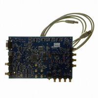
CDB42L55 Cirrus Logic Inc, CDB42L55 Datasheet - Page 10

CDB42L55
Manufacturer Part Number
CDB42L55
Description
Eval Bd Ultra Low Power Stereo Codec
Manufacturer
Cirrus Logic Inc
Specifications of CDB42L55
Main Purpose
Audio, CODEC
Embedded
Yes, FPGA / CPLD
Utilized Ic / Part
CS42L55
Primary Attributes
2 Stereo Analog Inputs, Stereo Line and Headphone Outputs, S/PDIF Transmitter and Receiver
Secondary Attributes
GUI, USB, RS232, I2C Interfaces, USB or External or Battery Power Supply
Product
Audio Modules
Lead Free Status / RoHS Status
Contains lead / RoHS non-compliant
Lead Free Status / RoHS Status
Contains lead / RoHS non-compliant
Other names
598-1506
CDB-42L55
CDB-42L55
10
2. TYPICAL CONNECTION DIAGRAM
+1.65 V to +3.47 V
Notes:
1. The headphone amplifier’s output power and distortion are rated using the nominal capacitance shown. Larger capacitance
reduces the ripple on the internal amplifiers’ supplies and in turn reduces the amplifier’s distortion at high output power levels.
Smaller capacitance may not sufficiently reduce ripple to achieve the rated output power and distortion. Since the actual value
of typical X7R/X5R ceramic capacitors deviates from the nominal value by a percentage specified in the manufacturer’s data
sheet, capacitors should be selected based on the minimum output power and maximum distortion required.
2. The headphone amplifier’s output power and distortion are rated using the nominal capacitance shown and using the default
charge pump switching frequency. The required capacitance follows an inverse relationship with the charge pump’s switching
frequency. When increasing the switching frequency, the capacitance may decrease; when lowering the switching frequency,
the capacitance must increase. Since the actual value of typical X7R/X5R ceramic capacitors deviates from the nominal value
by a percentage specified in the manufacturer’s data sheet, capacitors should be selected based on the minimum output
power, maximum distortion and maximum charge pump switching frequency required.
3. Additional bulk capacitance may be added to improve PSRR at low frequencies.
4. These capacitors serve as a charge reservoir for the internal switched capacitor ADC modulators and should be placed as
close as possible to the inputs. They are only needed when the PGA (Programmable Gain Amplifier) is bypassed.
5. Input pairs (such as AIN2A, AIN2REF and AIN2B) may be left floating if they are not used.
+1.65 V to +2.71 V
Digital Audio
Processor
2 k
Ω
**
2.2 µF
2.2 µF
2.2 µF
2.2 µF
2.2 µF
Note 2
Note 1
2 k
Note 1
Ω
0.1 µF
**
**
**
Figure 1. Typical Connection Diagram
**
**
1 µF
-VHPFILT
FLYP
FLYC
FLYN
MCLK
SCLK
LRCK
SDIN
SDOUT
RESET
SCL
SDA
+VHPFILT
VCP
VL
**
VDFILT
GND/Thermal Pad
CS42L55
VLDO
**
0.1 µF
HPDETECT
LINEOUTA
LINEOUTB
LINEREF
AIN1REF
AIN2REF
HPOUTB
HPOUTA
AFILTA
AFILTB
VA
HPREF
AGND
AIN1A
AIN1B
AIN2A
AIN2B
FILT+
**
VQ
0.1 µF
0.1 µF
0.1 µF
1 µF
1 µF
**
**
562 Ω
562 Ω
**
**
1000 pF
*
33 Ω
33 Ω
1800 pF
1800 pF
1800 pF
1800 pF
47 kΩ
3300 pF
*
*
3300 pF
Note 4
1000 pF
*
*
*
*
**
*
*
LPF is Optional
Low ESR, X7R/X5R dielectric capacitors.
NPO/C0G dielectric capacitors.
1 µF
1 µF
1 µF
1 µF
**
**
**
**
+1.65 V to +2.71 V
Note 3
100 Ω
100 Ω
100 Ω
100 Ω
**
2.2 µF
100 kΩ
100 kΩ
100 kΩ
100 kΩ
2.2 µF
**
Headphone Out
Left & Right
R
R
Analog
Input 1
ext
ext
Analog
Input 2
Line Level Out
Left & Right
Note 5
CS42L55
DS773F1


