CDB42L55 Cirrus Logic Inc, CDB42L55 Datasheet
CDB42L55
Specifications of CDB42L55
CDB-42L55


Related parts for CDB42L55


CDB42L55 Summary of contents
Page 1
Ultra Low Power, Stereo CODEC w/Class H Headphone Amp DIGITAL to ANALOG FEATURES 5 mW Stereo Playback Power Consumption 99 dB Dynamic Range (A-wtd) -86 dB THD+N Digital Signal Processing Engine – Bass & Treble Tone Control, De-Emphasis – Master ...
Page 2
... The CS42L55 is available in a 36-pin QFN package for the Commercial (-40°C to +85°C) grade. The CDB42L55 Customer Demonstration board is also available for device evaluation and implementation sug- gestions. Please see “Ordering Information” on page 73 for complete details ...
Page 3
TABLE OF CONTENTS 1. PIN DESCRIPTIONS .............................................................................................................................. 8 1.1 I/O Pin Characteristics ...................................................................................................................... 9 2. TYPICAL CONNECTION DIAGRAM ................................................................................................... 10 3. CHARACTERISTIC AND SPECIFICATION TABLES ......................................................................... 11 RECOMMENDED OPERATING CONDITIONS ................................................................................... 11 ABSOLUTE MAXIMUM RATINGS ....................................................................................................... 11 ANALOG INPUT CHARACTERISTICS ...
Page 4
REGISTER QUICK REFERENCE ........................................................................................................ 40 6. REGISTER DESCRIPTION .................................................................................................................. 42 6.1 Fab I.D. and Revision Register (Address 01h) (Read Only) ........................................................... 42 6.1.1 Chip Revision (Read Only) .................................................................................................... 42 6.2 Power Control 1 (Address 02h) ...................................................................................................... 42 6.2.1 Power ...
Page 5
Invert PCM Signal Polarity .................................................................................................. 51 6.13.5 Master Playback Mute ......................................................................................................... 51 6.14 ADCx Mixer Volume: ADCA (Address 10h) & ADCB (Address 11h) ...................................................................................... 51 6.14.1 ADC Mixer Channel x Mute ................................................................................................. 51 6.14.2 ADC Mixer Channel x Volume ...
Page 6
ALC Release Rate (Address 25h) ................................................................................................ 63 6.30.1 ALC Release Rate ............................................................................................................... 63 6.31 ALC Threshold (Address 26h) ...................................................................................................... 64 6.31.1 ALC Maximum Threshold .................................................................................................... 64 6.31.2 ALC Minimum Threshold ..................................................................................................... 64 6.32 Noise Gate Control (Address 27h) ............................................................................................... ...
Page 7
Figure 18.Beep Configuration Options ...................................................................................................... 32 Figure 19.Peak Detect & Limiter ............................................................................................................... 33 Figure 20.I²S Format ................................................................................................................................. 34 Figure 21.Control Port Timing, I²C Write ................................................................................................... 38 Figure 22.Control Port Timing, I²C Read ................................................................................................... 38 Figure 23.PGA Step Size vs. Volume ...
Page 8
PIN DESCRIPTIONS SDIN LRCK FLYP +VHPFILT FLYC FLYN Pin Name # SDIN 1 Serial Audio Data Input (Input) - Input for two’s complement serial audio data. Left Right Clock (Input/Output) - Determines which channel, Left or Right, is currently ...
Page 9
VA 17 Analog Power (Input) - Power supply for the internal analog section. AGND 18 Analog Ground (Input) - Ground reference for the internal analog section. FILT+ 19 Positive Voltage Reference (Output) - Positive reference voltage for the internal sampling ...
Page 10
TYPICAL CONNECTION DIAGRAM 2.2 µF Note 1 +1. +2.71 V 2.2 µF Note 2 2.2 µF 2.2 µF Note 1 2.2 µF Digital Audio Processor Ω +1. +3. Notes: ...
Page 11
CHARACTERISTIC AND SPECIFICATION TABLES RECOMMENDED OPERATING CONDITIONS GND = AGND = 0 V, all voltages with respect to ground. Parameters DC Power Supply Analog Charge Pump LDO Regulator for Digital Serial/Control Port Interface Ambient Temperature ABSOLUTE MAXIMUM RATINGS GND ...
Page 12
ANALOG INPUT CHARACTERISTICS Test Conditions (unless otherwise specified): Connections to the CS42L55 are shown in the gram" on page 10; Input kHz sine wave through the passive input filter, PGA = 0 dB; All Supplies = VA; ...
Page 13
ADC DIGITAL FILTER CHARACTERISTICS Parameter Frequency Response ( kHz) Passband Stopband Stopband Attenuation Total Group Delay High-Pass Filter Characteristics (48 kHz Fs) Passband Passband Ripple Phase Deviation @ 20 Hz Filter Settling Time (Note 10) Notes: 8. ...
Page 14
HP OUTPUT CHARACTERISTICS Test conditions (unless otherwise specified): Connections to the CS42L55 are shown in the page 10; Input test signal is a full-scale 997 Hz sine wave; All Supplies = VA, VCP Mode; GND = AGND = 0 V; ...
Page 15
LINE OUTPUT CHARACTERISTICS Test conditions (unless otherwise specified): Connections to the CS42L55 are shown in the page 10; Input test signal is a full-scale 997 Hz sine wave; All Supplies = VA, VCP Mode; GND = AGND = 0 V; ...
Page 16
ANALOG PASSTHROUGH CHARACTERISTICS Test Conditions (unless otherwise specified): Connections to the CS42L55 are shown in the page 10; Input kHz sine wave through the passive input filter shown in plies = VA, VCP Mode; GND = AGND ...
Page 17
SWITCHING SPECIFICATIONS - SERIAL PORT Inputs: Logic 0 = GND = AGND, Logic 1 = VL, LRCK, SCLK, SDOUT C Parameters RESET pin Low Pulse Width MCLK Frequency MCLK Duty Cycle Slave Mode (Figure 5) Input Sample Rate (LRCK) LRCK ...
Page 18
SWITCHING SPECIFICATIONS - CONTROL PORT Inputs: Logic 0 = GND = AGND, Logic 1 = VL, SDA C Parameter SCL Clock Frequency RESET Rising Edge to Start Bus Free Time Between Transmissions Start Condition Hold Time (prior to first clock ...
Page 19
POWER SUPPLY REJECTION (PSRR) CHARACTERISTICS Test Conditions (unless otherwise specified): Connections to the CS42L55 are shown in the page 10; GND = AGND = 0 V; all voltages with respect to ground. Parameters PSRR with 100 mVpp, 1 kHz signal ...
Page 20
POWER CONSUMPTION - ALL SUPPLIES = 1.8 V Power Ctl. Registers 02h page 42 Operation Test Condi- tions (unless otherwise specified): All zeros input, slave mode, sample rate = 48 kHz; No load. Refer to Figure 8 on page 19. ...
Page 21
POWER CONSUMPTION - ALL SUPPLIES = 2.5 V Power Ctl. Registers MUX Registers 02h page 42 Operation Test Condi- tions (unless otherwise specified): /All zeros input, slave mode, sample rate = 48 kHz; No load. Refer to Figure 8 on ...
Page 22
APPLICATIONS 4.1 Overview 4.1.1 Basic Architecture The CS42L55 is a highly integrated, ultra-low power, 24-bit audio CODEC comprised of stereo A/D and D/A converters with pseudo-differential stereo input and output amplifiers. The ADC and DAC are de- signed using ...
Page 23
Analog Inputs DIGSUM[1:0] Swap/ Mix DIGMUX Referenced Control Register Location Analog Front End PGAxMUX “PGA x Input Select” on page 49 PDN_ADCx “Power Down ADC x” on page 42 PGAxVOL[5:0] “PGAx Volume” on page 49 PGAB=A “PGA Channel B=A” ...
Page 24
Pseudo-Differential Inputs The CS42L55 implements a pseudo-differential input stage. The AINxREF inputs are intended to be used as a pseudo-differential reference signal. This feature provides 0 noise rejection with single-ended sig- nals. Figure 10 shows a basic diagram outlining ...
Page 25
Referenced Control PGAxVOL[5:0] ..................... ADCxATT[7:0] ...................... MAX[2:0], MIN[2:0] .............. Input (before ALC) MIN[2:0] below full scale ALC Response Output (after ALC) MIN[2:0] below full scale 4.3 Analog In to Analog Out Passthrough The CS42L55 accommodates analog routing of the analog ...
Page 26
Analog Outputs INPUTS FROM ADCA and ADCB PMIXAMUTE PMIXBMUTE PMIXAVOL[6:0] PMIXBVOL[6:0] Demph INV_PCMA DEEMPH INV_PCMB OFFTIME[2:0] ONTIME[3:0] FREQ[3:0] BEEP[1:0] Digital Mix to ADC Serial Interface Referenced Control Register Location DSP PDN_DSP “Power Down DSP” on page 50 DEEMPH “HP/Line ...
Page 27
VCP from PGAx from DACx Referenced Control Register Location Analog Output ADPTPWR[1:0] “Adaptive Power Adjustment” on page 45 CHGFREQ[3:0] “Charge Pump Frequency” on page 67 PDN_HPx[1:0] “Headphone Power Control” on page 43 PDN_LINx[1:0] “Line Power Control” on page 43 HPxMUTE ...
Page 28
Standard Class AB Operation (Mode 01 and 10) When the Adaptive Power bits are set to either 01 or 10, the rail voltages supplied to the amplifiers will be held to ±VCP/2 or ±VCP, respectively. For these two settings, ...
Page 29
Referenced Control HPxVOL[7:0] ....................... LINExVOL[7:0] .................... MSTxVOL[7:0]..................... MSTxMUTE......................... AMIXxVOL[6:0].................... PMIXxVOL[6:0].................... AINADV[7:0] ........................ DINADV[7:0]........................ BOOSTx .............................. ADCxMUX ........................... PGAxVOL............................ ADCxMUTE......................... ADCxSWP........................... PCMxSWP .......................... HPxMUX.............................. LINExMUX........................... HPxMUTE ........................... LINExMUTE ........................ PDN_HPx ............................ PDN_LINEx ......................... TREB................................... BASS................................... TCEN................................... BEEP................................... BPVOL ................................ ADCB=A .............................. ...
Page 30
When the charge pump transitions from the higher set of rail voltages to the lower set, there is a one sec- ond delay before the charge pump supplies the lower rail voltages to the ...
Page 31
Efficiency As discussed in previous sections, the amplifiers internal to the CS42L55 operate from one of two sets of rail voltages, based upon the needs of the signal being amplified or the total gain/attenuation settings. The power curves for ...
Page 32
CONTINUOUS BEEP: Beep turns configurable frequency (FREQ) and volume (BPVOL) and remains on BEEP[1:0] = until REPEAT is cleared. '11' MULTI-BEEP: Beep turns configurable frequency (FREQ) BEEP[1:0] = and volume (BPVOL) for the duration ...
Page 33
Input MAX[2:0] Limiter Volume Output (after Limiter) MAX[2:0] DS773F1 ATTACK/RELEASE SOUND CUSHION ARATE[5:0] RRATE[5:0] Figure 19. Peak Detect & Limiter CS42L55 CUSH[2:0] 33 ...
Page 34
Serial Port Clocking The CODEC serial audio interface port operates either as a slave or master. It accepts externally generated clocks in Slave Mode (M/S = ‘0’b) and will generate synchronous clocks derived from an input master clock (MCLK) ...
Page 35
After the PDN bit is released and MCLK is valid, the quiescent voltage, VQ, and the internal voltage refer- ence, FILT+, will begin powering up to normal operation. The charge pump slowly powers up and charges the capacitors. Power is ...
Page 36
Recommended Power-Down Sequence 1. To minimize pops on the headphone or line amplifier, each respective analog volume control must first be muted and set to maximum attenuation. Register Controls: HPxMUTE, LINExMUTE, HPxVOL[6:0], LINExVOL[6:0] 2. Set the PDN bit to ...
Page 37
The zero cross timeout, however, is dependent on the serial port clock domain. Thus, to fully power down, the ADC must briefly power up to enable the zero cross state machine. Follow the remaining steps below to complete the ...
Page 38
Control Port Operation The control port is used to access the registers allowing the CODEC to be configured for the desired oper- ational modes and formats. The operation of the control port may be completely asynchronous with respect to ...
Page 39
Receive acknowledge bit. Send stop condition, aborting write. Send start condition. Send 10010101 (chip address & read operation). Receive acknowledge bit. Receive byte, contents of selected register. Send acknowledge bit. Send stop condition. Setting the auto-increment bit in the MAP ...
Page 40
REGISTER QUICK REFERENCE Default values are shown below the bit names ( I²C Address: 1001010[R/W] - 10010100 = 0x94(Write); 10010101 = 0x95(Read) Adr. Function 7 01h ID Reserved Reserved p 42 (Read Only) x 02h Reserved Reserved Power Ctl ...
Page 41
I²C Address: 1001010[R/W] - 10010100 = 0x94(Write); 10010101 = 0x95(Read) Adr. Function 7 1Bh Headphone B HPBMUTE HPBVOL6 p 57 Volume 0 1Ch Line A LINEAMUTE LINEAVOL6 p 58 Volume 0 1Dh Line B LINEBMUTE LINEBVOL6 p 58 Volume 0 ...
Page 42
REGISTER DESCRIPTION Except for the chip I.D., revision register, and status register, which are Read Only, all registers are Read/Write. See the following bit definition tables for bit assignment information. The default state of each bit after a power-up ...
Page 43
Power Control 2 (Address 03h PDN_HPB1 PDN_HPB0 PDN_HPA1 6.3.1 Headphone Power Control Configures how the HPDETECT pin, 29, controls the power for the headphone amplifier. PDN_HPx[1:0] Headphone Status Headphone channel is ON when the HPDETECT pin, 29, ...
Page 44
SCLK Equals MCLK Configures the SCLK signal source and speed for master mode. SCK=MCK[1:0] Output SCLK 00 Re-timed, bursted signal with minimal speed needed to clock the required data samples 01 Reserved 10 MCLK signal after the MCLK divide ...
Page 45
Sample Rate Group Specifies whether or not the input/output sample rate is 8 kHz, 16 kHz or 32 kHz. 32kGROUP 8 kHz, 16 kHz or 32 kHz sample rate Yes Application: “Serial Port Clocking” ...
Page 46
Analog Zero Cross Configures when the signal level changes occur for the analog volume controls. ANLGZCx Volume Changes Do not occur on a zero cross- 0 ing 1 Occur on a zero crossing Note: If the signal does not ...
Page 47
Line Input Select Selects the specified analog input signal into line amplifier x. LINExMUX Selected Input to Line Amplifier Ch DACx 1 PGAx - Use PGAxMUX bit Note: The PGA path must not be selected while the ...
Page 48
Misc. ADC Control (Address 0Ah ADCB=A PGAB=A DIGSUM1 6.10.1 ADC Channel B=A Configures independent or ganged volume control of the ADC and the ALC. ADCB=A Single Volume Control 0 Disabled 1 Enabled 6.10.2 PGA Channel B=A Configures ...
Page 49
PGA x MUX, Volume: PGA A (Address 0Bh) & PGA B (Address 0Ch BOOSTx PGAxMUX PGAxVOL5 6.11.1 Boostx Configures a +20 dB boost on channel x. BOOSTx +20 dB Boost 0 No boost applied 1 +20 ...
Page 50
ADCx Attenuator Control: ADCAATT (Address 0Dh) & ADCBATT (Address 0Eh ADCxATT7 ADCxATT6 ADCxATT5 6.12.1 ADCx Volume Sets the volume of the ADC signal. ADCxATT[7:0] Volume 0111 1111 0 dB ... ... 0000 0000 0 dB 1111 1111 ...
Page 51
Invert PCM Signal Polarity Configures the polarity of the digital input signal. INV_PCMx PCM Signal Polarity 0 Not Inverted 1 Inverted 6.13.5 Master Playback Mute Configures a digital mute on the master volume control for channel x. MSTxMUTE Master ...
Page 52
PCMx Mixer Volume: PCMA (Address 12h) & PCMB (Address 13h PMIXxMUTE PMIXxVOL6 PMIXxVOL5 6.15.1 PCM Mixer Channel x Mute Configures a digital mute on the PCM mix from the serial data input (SDIN) to the DSP Engine. ...
Page 53
Beep Frequency & On Time (Address 14h FREQ3 FREQ2 FREQ1 6.16.1 Beep Frequency Sets the frequency of the beep signal. FREQ[3:0] Frequency ( kHz) 0000 254.76 Hz 0001 509.51 Hz 0010 571.65 ...
Page 54
Beep On Time Sets the on duration of the beep signal. ONTIME[3:0] On Time ( kHz) 0000 ~86 ms 0001 ~430 ms 0010 ~780 ms 0011 ~1.20 s 0100 ~1.50 s 0101 ~1.80 s ...
Page 55
Beep Volume Sets the volume of the beep signal. BPVOL[4:0] Gain 00110 +12.0 dB ··· ··· 00000 0 dB 11111 -2 dB 11110 -4 dB ··· ··· 00111 -50 dB Step Size Application: “Beep Generator” on page ...
Page 56
Bass Corner Frequency Sets the corner frequency for the bass shelving filter. BASSCF[1:0] Bass Corner Frequency Setting 100 Hz 10 200 Hz 11 250 Hz 6.18.4 Tone Control Enable Configures the treble and bass activation. ...
Page 57
Master Volume Control: MSTA (Address 18h) & MSTB (Address 19h MSTxVOL7 MSTxVOL6 MSTxVOL5 6.20.1 Master Volume Control Sets the volume of the signal out the DSP. MSTxVOL[7:0] Master Volume 0001 1000 +12.0 dB ··· ··· 0000 0000 ...
Page 58
Line Volume Control: LINEA (Address 1Ch) & LINEB (Address 1Dh LINExMUTE LINExVOL6 LINExVOL5 6.22.1 Line Channel x Mute Configures an analog mute on the line amplifier. LINExMUTE HP Amp Mute 0 Disabled 1 Enabled 6.22.2 Line Volume ...
Page 59
Analog Input Advisory Volume (Address 1Eh AINADV7 AINADV6 AINADV5 6.23.1 Analog Input Advisory Volume Defines the maximum analog input volume level used by the class H controller to determine the appropri- ate supply for the HP and ...
Page 60
ADC & PCM Channel Mixer (Address 20h PCMBSWP1 PCMBSWP0 PCMASWP1 6.25.1 PCM Mix Channel Swap Configures a mix/swap of the PCM Mix to the headphone/line outputs. PCMxSWP[1:0] PCM Mix to HP/LINEOUTA 00 Left 01 (Left + Right)/2 ...
Page 61
Limiter Cushion Threshold Sets the minimum level at which to disengage the Limiter’s attenuation at the release rate (LIMRRATE - “Limiter Release Rate” on page CUSH[2:0] Threshold Setting 000 0 dB 001 -3 dB 010 -6 dB 011 -9 ...
Page 62
Limiter Release Rate Sets the rate at which the limiter releases the digital attenuation from levels below the CUSH[2:0] thresh- old (“Limiter Cushion Threshold” on page (“Master Volume Control” on page LIMRRATE[5:0] Release Time 00 0000 Fastest Release ··· ...
Page 63
ALC Attack Rate Sets the rate at which the ALC applies analog and/or digital attenuation from levels above the AMAX[2:0] threshold (“ALC Maximum Threshold” on page ALCARATE[5:0] Attack Time 00 0000 Fastest Attack ··· ··· 11 1111 Slowest Attack ...
Page 64
ALC Threshold (Address 26h ALCMAX2 ALCMAX1 ALCMAX0 6.31.1 ALC Maximum Threshold Sets the maximum level, below full-scale, at which to limit and attenuate the input signal at the attack rate (ALCARATE - “ALC Attack Rate” on page ...
Page 65
Noise Gate Enable Configures the noise gate. NG Noise Gate Status 0 Disabled 1 Enabled 6.32.3 Noise Gate Threshold and Boost THRESH sets the threshold level of the noise gate. Input signals below the threshold level will be attenu- ...
Page 66
Limiter Soft Ramp Disable Configures an override of the digital soft ramp setting. LIMSRDIS Limiter Soft Ramp Disable 0 OFF; Limiter Attack Rate is dictated by the DIGSFT 1 ON; Limiter volume changes take effect in one step, regardless ...
Page 67
ADCx Overflow (Read Only) Indicates the over-range status in the ADC signal path. ADCxOVFL ADC Overflow Status clipping has occurred anywhere in the ADC signal path. 1 Clipping has occurred in the ADC signal path. 6.35 Charge ...
Page 68
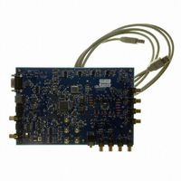
... FILT+ and VQ pins in order to avoid unwanted coupling into the modulators. The FILT+, VQ, +VHPFILT and -VHPFILT capacitors must be positioned to minimize the electrical path from each re- spective pin to AGND. The CDB42L55 evaluation board demonstrates the optimum layout and power sup- ply arrangements. ...
Page 69
ANALOG VOLUME NON-LINEARITY (DNL & INL) 0.52 0.5 0.48 0.46 0.44 0.42 0 PGA Volume Setting Figure 23. PGA Step Size vs. Volume Setting -60 -50 -40 -30 ...
Page 70
ADC & DAC DIGITAL FILTERS 0.25 0.2 0.15 0.1 0.05 0 −0.05 −0.1 −0.15 −0.2 −0.25 0 0.05 0.1 0.15 0.2 0.25 0.3 Frequency (normalized to Fs) Figure 27. ADC Passband Ripple 0 −10 −20 −30 −40 −50 −60 ...
Page 71
DEFINITIONS Dynamic Range The ratio of the rms value of the signal to the rms sum of all other spectral components over the specified bandwidth. Dynamic Range is a signal-to-noise ratio measurement over the specified band width made with ...
Page 72
DIMENSIONS (Unless otherwise specified, linear tolerance is ±0.05 mm, and angular tolerance is ±2 deg.) 36L QFN ( BODY) PACKAGE DRAWING D 1.50 REF Pin #1 IDENTIFIER LASER MARKING INCHES Dim MIN A 0.01773 A1 0.00000 ...
Page 73
... INFORMATION Product Description Ultra Low Power, Stereo CS42L55 CODEC w/ Class H HP Amp for Portable Apps CDB42L55 CS42L55 Evaluation Board 13.REFERENCES 1. Philips Semiconductor, The I²C-Bus Specification: Version 2.1, January 2000. http://www.semiconductors.philips.com 14.REVISION HISTORY Revision F1 Initial Release Contacting Cirrus Logic Support For all product questions and inquiries contact a Cirrus Logic Sales Representative ...