CDB42L55 Cirrus Logic Inc, CDB42L55 Datasheet - Page 11
CDB42L55
Manufacturer Part Number
CDB42L55
Description
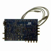
Eval Bd Ultra Low Power Stereo Codec
Manufacturer
Cirrus Logic Inc
Specifications of CDB42L55
Main Purpose
Audio, CODEC
Embedded
Yes, FPGA / CPLD
Utilized Ic / Part
CS42L55
Primary Attributes
2 Stereo Analog Inputs, Stereo Line and Headphone Outputs, S/PDIF Transmitter and Receiver
Secondary Attributes
GUI, USB, RS232, I2C Interfaces, USB or External or Battery Power Supply
Product
Audio Modules
Lead Free Status / RoHS Status
Contains lead / RoHS non-compliant
Lead Free Status / RoHS Status
Contains lead / RoHS non-compliant
Other names
598-1506
CDB-42L55
CDB-42L55


DS773F1
3. CHARACTERISTIC AND SPECIFICATION TABLES
RECOMMENDED OPERATING CONDITIONS
GND = AGND = 0 V, all voltages with respect to ground.
ABSOLUTE MAXIMUM RATINGS
GND = AGND = 0 V; all voltages with respect to ground.
Notes:
WARNING: Operation at or beyond these limits may result in permanent damage to the device. Normal operation
DC Power Supply
Analog
Charge Pump
LDO Regulator for Digital
Serial/Control Port Interface
Ambient Temperature
DC Power Supply
Input Current
Analog Input Voltage
Digital Input Voltage
Ambient Operating Temperature (power applied)
Storage Temperature
1. Due to the existence of parasitic body diodes between VCP and VA, current flows from VCP to VA when-
2. Any pin except supplies. Transient currents of up to ±100 mA on the analog input pins will not cause
3. The maximum over/under voltage is limited by the input current.
ever the VA power supply is lower than VCP. This causes a “back-powering” effect on the VA power
supply rails internal to the part. Hence VA should be maintained at an equal or greater voltage than VCP
at all times. While “back-powering” does not have any adverse effects on device operation with respect
to performance and reliability, it does lead to extra power consumption and therefore should be avoided.
SCR latch-up.
is not guaranteed at these extremes.
Parameters
Parameters
Analog, Charge Pump, LDO
Serial/Control Port Interface
Commercial - CNZ
(Note 2)
(Note 3)
(Note 3)
VA, VCP, VLDO
Symbol
Symbol
V
T
V
VLDO
VL
T
I
IND
VCP
stg
in
IN
A
VA
VL
T
A
AGND-0.7
1.65
1.65
1.65
Min
Min
1.65
-0.3
-0.3
-0.3
-40
-50
-65
-
VA+0.7
VL+0.4
Max
Max
+115
+150
2.71
2.71
3.47
+85
±10
3.0
4.0
VA
CS42L55
Units
Units
mA
°C
°C
°C
V
V
V
V
V
V
V
V
11
Related parts for CDB42L55
Image
Part Number
Description
Manufacturer
Datasheet
Request
R

Part Number:
Description:
Development Kit
Manufacturer:
Cirrus Logic Inc
Datasheet:
Part Number:
Description:
Development Kit
Manufacturer:
Cirrus Logic Inc
Datasheet:


Part Number:
Description:
High-efficiency PFC + Fluorescent Lamp Driver Reference Design
Manufacturer:
Cirrus Logic Inc
Datasheet:
Part Number:
Description:
Development Kit
Manufacturer:
Cirrus Logic Inc
Datasheet:
Part Number:
Description:
Development Kit
Manufacturer:
Cirrus Logic Inc
Datasheet:

Part Number:
Description:
Development Kit
Manufacturer:
Cirrus Logic Inc
Datasheet:
Part Number:
Description:
Development Kit
Manufacturer:
Cirrus Logic Inc
Datasheet:
Part Number:
Description:
Development Kit
Manufacturer:
Cirrus Logic Inc
Datasheet:
Part Number:
Description:
Development Kit
Manufacturer:
Cirrus Logic Inc
Datasheet:

Part Number:
Description:
EVALUATION BOARD FOR CS8427
Manufacturer:
Cirrus Logic Inc
Datasheet:

Part Number:
Description:
BOARD EVAL FOR CS8416 RCVR
Manufacturer:
Cirrus Logic Inc
Datasheet:

Part Number:
Description:
EVALUATION BOARD FOR CS8420
Manufacturer:
Cirrus Logic Inc
Datasheet:

Part Number:
Description:
KIT DEVELOPMENT EP9315 ARM9
Manufacturer:
Cirrus Logic Inc
Datasheet:

Part Number:
Description:
KIT DEVELOPMENT EP9302 ARM9
Manufacturer:
Cirrus Logic Inc
Datasheet: