PIC16F689-E/ML Microchip Technology, PIC16F689-E/ML Datasheet - Page 297
PIC16F689-E/ML
Manufacturer Part Number
PIC16F689-E/ML
Description
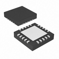
IC,MICROCONTROLLER,8-BIT,PIC CPU,CMOS,LLCC,20PIN,PLASTIC
Manufacturer
Microchip Technology
Series
PIC® 16Fr
Datasheets
1.PIC16F616T-ISL.pdf
(8 pages)
2.PIC16F690DM-PCTLHS.pdf
(306 pages)
3.PIC16F677-IP.pdf
(2 pages)
4.PIC16F677-IP.pdf
(16 pages)
Specifications of PIC16F689-E/ML
Rohs Compliant
YES
Core Processor
PIC
Core Size
8-Bit
Speed
20MHz
Connectivity
I²C, SPI, UART/USART
Peripherals
Brown-out Detect/Reset, POR, WDT
Number Of I /o
18
Program Memory Size
7KB (4K x 14)
Program Memory Type
FLASH
Eeprom Size
256 x 8
Ram Size
256 x 8
Voltage - Supply (vcc/vdd)
2 V ~ 5.5 V
Data Converters
A/D 12x10b
Oscillator Type
Internal
Operating Temperature
-40°C ~ 125°C
Package / Case
20-VQFN Exposed Pad, 20-HVQFN, 20-SQFN, 20-DHVQFN
Lead Free Status / RoHS Status
Lead free / RoHS Compliant
For Use With
AC164324 - MODULE SKT FOR MPLAB 8DFN/16QFNAC162061 - HEADER INTRFC MPLAB ICD2 20PIN
Lead Free Status / RoHS Status
Lead free / RoHS Compliant


INDEX
A
A/D
Absolute Maximum Ratings .............................................. 231
AC Characteristics
ACK pulse ......................................................................... 188
ADC .................................................................................. 107
ADCON0 Register............................................................. 113
ADCON1 Register............................................................. 114
ADRESH Register (ADFM = 0) ......................................... 115
ADRESH Register (ADFM = 1) ......................................... 115
ADRESL Register (ADFM = 0).......................................... 115
ADRESL Register (ADFM = 1).......................................... 115
Analog Input Connection Considerations.......................... 100
Analog-to-Digital Converter. See ADC
ANSEL Register .................................................................. 61
ANSELH Register ............................................................... 61
Assembler
B
BAUDCTL Register ........................................................... 162
BF bit................................................................................. 180
Block Diagrams
© 2008 Microchip Technology Inc.
Specifications............................................ 255, 256, 257
Industrial and Extended ............................................ 241
Load Conditions ........................................................ 240
Acquisition Requirements ......................................... 116
Associated registers.................................................. 118
Block Diagram........................................................... 107
Calculating Acquisition Time..................................... 116
Channel Selection..................................................... 108
Configuration............................................................. 108
Configuring Interrupt ................................................. 111
Conversion Clock...................................................... 108
Conversion Procedure .............................................. 111
Internal Sampling Switch (R
Interrupts................................................................... 109
Operation .................................................................. 111
Operation During Sleep ............................................ 111
Port Configuration ..................................................... 108
Reference Voltage (V
Result Formatting...................................................... 110
Source Impedance.................................................... 116
Special Event Trigger................................................ 111
Starting an A/D Conversion ...................................... 110
MPASM Assembler................................................... 228
(CCP) Capture Mode Operation ............................... 128
ADC .......................................................................... 107
ADC Transfer Function ............................................. 117
Analog Input Model ........................................... 100, 117
Auto-Shutdown ......................................................... 141
CCP PWM................................................................. 130
Clock Source............................................................... 47
Comparator C1 ........................................................... 94
Comparator C2 ........................................................... 94
Compare ................................................................... 129
Crystal Operation ........................................................ 50
EUSART Receive ..................................................... 152
EUSART Transmit .................................................... 151
External RC Mode....................................................... 51
Fail-Safe Clock Monitor (FSCM) ................................. 57
In-Circuit Serial Programming Connections.............. 216
Interrupt Logic ........................................................... 209
On-Chip Reset Circuit ............................................... 200
PIC16F631.................................................................... 9
REF
)......................................... 108
SS
) Impedance.............. 116
PIC16F631/677/685/687/689/690
Break Character (12-bit) Transmit and Receive ............... 169
Brown-out Reset (BOR).................................................... 202
C
C Compilers
Capture Module. See Enhanced Capture/Compare/
Capture/Compare/PWM (CCP)
CCPxCON (Enhanced) Register ...................................... 127
CKE bit ............................................................................. 180
PIC16F677 ................................................................. 10
PIC16F685 ................................................................. 11
PIC16F687/689 .......................................................... 12
PIC16F690 ................................................................. 13
PWM (Enhanced) ..................................................... 133
RA0 Pins..................................................................... 64
RA1 Pins..................................................................... 65
RA2 Pin ...................................................................... 65
RA3 Pin ...................................................................... 66
RA4 Pin ...................................................................... 66
RA5 Pin ...................................................................... 67
RB4 Pin ...................................................................... 71
RB5 Pin ...................................................................... 72
RB6 Pin ...................................................................... 73
RB7 Pin ...................................................................... 74
RC0 and RC1 Pins ..................................................... 77
RC2 and RC3 Pins ..................................................... 77
RC4 Pin ...................................................................... 78
RC5 Pin ...................................................................... 78
RC6 Pin ...................................................................... 79
RC7 Pin ...................................................................... 79
Resonator Operation .................................................. 50
SSP (I
SSP (SPI Mode) ....................................................... 179
Timer1 ........................................................................ 84
Timer2 ........................................................................ 91
TMR0/WDT Prescaler ................................................ 81
Watchdog Timer (WDT)............................................ 212
Associated ................................................................ 203
Specifications ........................................................... 245
Timing and Characteristics ....................................... 244
MPLAB C18.............................................................. 228
MPLAB C30.............................................................. 228
PWM(ECCP)
Associated registers w/ Capture/Compare/PWM ..... 149
Capture Mode........................................................... 128
CCPx Pin Configuration............................................ 128
Compare Mode......................................................... 129
Prescaler .................................................................. 128
PWM Mode............................................................... 130
PWM Period ............................................................. 131
Setup for PWM Operation ........................................ 132
CCPx Pin Configuration.................................... 129
Software Interrupt Mode ........................... 128, 129
Special Event Trigger ....................................... 129
Timer1 Mode Selection............................. 128, 129
Duty Cycle ........................................................ 131
Effects of Reset ................................................ 132
Example PWM Frequencies and
Example PWM Frequencies and
Operation in Sleep Mode.................................. 132
Setup for Operation .......................................... 132
System Clock Frequency Changes .................. 132
2
C Mode)........................................................ 188
Resolutions, 20 MHZ ................................ 131
Resolutions, 8 MHz .................................. 131
DS41262E-page 295
Related parts for PIC16F689-E/ML
Image
Part Number
Description
Manufacturer
Datasheet
Request
R

Part Number:
Description:
IC PIC MCU FLASH 4KX14 20SSOP
Manufacturer:
Microchip Technology
Datasheet:

Part Number:
Description:
IC PIC MCU FLASH 4KX14 20SOIC
Manufacturer:
Microchip Technology
Datasheet:

Part Number:
Description:
IC PIC MCU FLASH 4KX14 20QFN
Manufacturer:
Microchip Technology
Datasheet:

Part Number:
Description:
IC PIC MCU FLASH 4KX14 20DIP
Manufacturer:
Microchip Technology
Datasheet:
Part Number:
Description:
IC PIC MCU FLASH 4KX14 20DIP
Manufacturer:
Microchip Technology
Datasheet:

Part Number:
Description:
IC,MICROCONTROLLER,8-BIT,PIC CPU,CMOS,SOP,20PIN,PLASTIC
Manufacturer:
Microchip Technology
Datasheet:
Part Number:
Description:
IC,MICROCONTROLLER,8-BIT,PIC CPU,CMOS,SSOP,20PIN,PLASTIC
Manufacturer:
Microchip Technology
Datasheet:
Part Number:
Description:
(PIC16F6xx) 20-Pin Flash Based / 8-Bit CMOS Microcontrollers
Manufacturer:
Microchip Technology

Part Number:
Description:
IC, 8BIT MCU, PIC16F, 32MHZ, SOIC-18
Manufacturer:
Microchip Technology
Datasheet:

Part Number:
Description:
IC, 8BIT MCU, PIC16F, 32MHZ, SSOP-20
Manufacturer:
Microchip Technology
Datasheet:
Part Number:
Description:
IC, 8BIT MCU, PIC16F, 32MHZ, DIP-18
Manufacturer:
Microchip Technology
Datasheet:

Part Number:
Description:
IC, 8BIT MCU, PIC16F, 32MHZ, QFN-28
Manufacturer:
Microchip Technology
Datasheet:

Part Number:
Description:
IC, 8BIT MCU, PIC16F, 32MHZ, QFN-28
Manufacturer:
Microchip Technology
Datasheet:
Part Number:
Description:
IC, 8BIT MCU, PIC16F, 32MHZ, QFN-28
Manufacturer:
Microchip Technology
Datasheet:
Part Number:
Description:
IC, 8BIT MCU, PIC16F, 32MHZ, SSOP-20
Manufacturer:
Microchip Technology
Datasheet: