PIC16F689-E/ML Microchip Technology, PIC16F689-E/ML Datasheet - Page 127
PIC16F689-E/ML
Manufacturer Part Number
PIC16F689-E/ML
Description
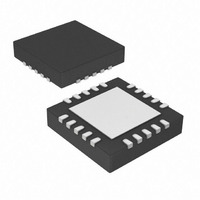
IC,MICROCONTROLLER,8-BIT,PIC CPU,CMOS,LLCC,20PIN,PLASTIC
Manufacturer
Microchip Technology
Series
PIC® 16Fr
Datasheets
1.PIC16F616T-ISL.pdf
(8 pages)
2.PIC16F690DM-PCTLHS.pdf
(306 pages)
3.PIC16F677-IP.pdf
(2 pages)
4.PIC16F677-IP.pdf
(16 pages)
Specifications of PIC16F689-E/ML
Rohs Compliant
YES
Core Processor
PIC
Core Size
8-Bit
Speed
20MHz
Connectivity
I²C, SPI, UART/USART
Peripherals
Brown-out Detect/Reset, POR, WDT
Number Of I /o
18
Program Memory Size
7KB (4K x 14)
Program Memory Type
FLASH
Eeprom Size
256 x 8
Ram Size
256 x 8
Voltage - Supply (vcc/vdd)
2 V ~ 5.5 V
Data Converters
A/D 12x10b
Oscillator Type
Internal
Operating Temperature
-40°C ~ 125°C
Package / Case
20-VQFN Exposed Pad, 20-HVQFN, 20-SQFN, 20-DHVQFN
Lead Free Status / RoHS Status
Lead free / RoHS Compliant
For Use With
AC164324 - MODULE SKT FOR MPLAB 8DFN/16QFNAC162061 - HEADER INTRFC MPLAB ICD2 20PIN
Lead Free Status / RoHS Status
Lead free / RoHS Compliant


10.2
Depending on the application, good programming
practice may dictate that the value written to the data
EEPROM should be verified (see Example 10-4) to the
desired value to be written.
EXAMPLE 10-4:
10.2.1
The data EEPROM is a high-endurance, byte
addressable array that has been optimized for the
storage of frequently changing information (e.g.,
program variables or other data that are updated often).
When variables in one section change frequently, while
variables in another section do not change, it is possible
to exceed the total number of write cycles to the
EEPROM (specification D124) without exceeding the
total number of write cycles to a single byte
(specifications D120 and D120A). If this is the case,
then a refresh of the array must be performed. For this
reason, variables that do not change (such as
constants, IDs, calibration, etc.) should be stored in
Flash program memory.
10.3
There are conditions when the user may not want to
write to the data EEPROM memory. To protect against
spurious EEPROM writes, various mechanisms have
been built in. On power-up, WREN is cleared. Also, the
Power-up
EEPROM write.
The write initiate sequence and the WREN bit together
help prevent an accidental write during:
• Brown-out
• Power Glitch
• Software Malfunction
10.4
Data memory can be code-protected by programming
the CPD bit in the Configuration Word register
(Register 14-1) to ‘0’.
© 2008 Microchip Technology Inc.
BANKSEL EEDAT
MOVF
BANKSEL EECON1
BSF
BANKSEL EEDAT
XORWF
BTFSS
GOTO
:
BANKSEL 0x00
Write Verify
Protection Against Spurious Write
Data EEPROM Operation During
Code-Protect
EEDAT, W
EECON1, RD
EEDAT, W
STATUS, Z
WRITE_ERR
USING THE DATA EEPROM
Timer
WRITE VERIFY
(64 ms
;
;EEDAT not changed
;from previous write
;
;YES, Read the
;value written
;
;
;Is data the same
;No, handle error
;Yes, continue
;Bank 0
duration)
PIC16F631/677/685/687/689/690
prevents
When the data memory is code-protected, only the CPU
is able to read and write data to the data EEPROM. It is
recommended to code-protect the program memory
when code-protecting data memory and programming
unused program memory with NOP instructions.
DS41262E-page 125
Related parts for PIC16F689-E/ML
Image
Part Number
Description
Manufacturer
Datasheet
Request
R

Part Number:
Description:
IC PIC MCU FLASH 4KX14 20SSOP
Manufacturer:
Microchip Technology
Datasheet:

Part Number:
Description:
IC PIC MCU FLASH 4KX14 20SOIC
Manufacturer:
Microchip Technology
Datasheet:

Part Number:
Description:
IC PIC MCU FLASH 4KX14 20QFN
Manufacturer:
Microchip Technology
Datasheet:

Part Number:
Description:
IC PIC MCU FLASH 4KX14 20DIP
Manufacturer:
Microchip Technology
Datasheet:
Part Number:
Description:
IC PIC MCU FLASH 4KX14 20DIP
Manufacturer:
Microchip Technology
Datasheet:

Part Number:
Description:
IC,MICROCONTROLLER,8-BIT,PIC CPU,CMOS,SOP,20PIN,PLASTIC
Manufacturer:
Microchip Technology
Datasheet:
Part Number:
Description:
IC,MICROCONTROLLER,8-BIT,PIC CPU,CMOS,SSOP,20PIN,PLASTIC
Manufacturer:
Microchip Technology
Datasheet:
Part Number:
Description:
(PIC16F6xx) 20-Pin Flash Based / 8-Bit CMOS Microcontrollers
Manufacturer:
Microchip Technology

Part Number:
Description:
IC, 8BIT MCU, PIC16F, 32MHZ, SOIC-18
Manufacturer:
Microchip Technology
Datasheet:

Part Number:
Description:
IC, 8BIT MCU, PIC16F, 32MHZ, SSOP-20
Manufacturer:
Microchip Technology
Datasheet:
Part Number:
Description:
IC, 8BIT MCU, PIC16F, 32MHZ, DIP-18
Manufacturer:
Microchip Technology
Datasheet:

Part Number:
Description:
IC, 8BIT MCU, PIC16F, 32MHZ, QFN-28
Manufacturer:
Microchip Technology
Datasheet:

Part Number:
Description:
IC, 8BIT MCU, PIC16F, 32MHZ, QFN-28
Manufacturer:
Microchip Technology
Datasheet:
Part Number:
Description:
IC, 8BIT MCU, PIC16F, 32MHZ, QFN-28
Manufacturer:
Microchip Technology
Datasheet:
Part Number:
Description:
IC, 8BIT MCU, PIC16F, 32MHZ, SSOP-20
Manufacturer:
Microchip Technology
Datasheet: