PIC16F689-E/ML Microchip Technology, PIC16F689-E/ML Datasheet - Page 182
PIC16F689-E/ML
Manufacturer Part Number
PIC16F689-E/ML
Description
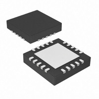
IC,MICROCONTROLLER,8-BIT,PIC CPU,CMOS,LLCC,20PIN,PLASTIC
Manufacturer
Microchip Technology
Series
PIC® 16Fr
Datasheets
1.PIC16F616T-ISL.pdf
(8 pages)
2.PIC16F690DM-PCTLHS.pdf
(306 pages)
3.PIC16F677-IP.pdf
(2 pages)
4.PIC16F677-IP.pdf
(16 pages)
Specifications of PIC16F689-E/ML
Rohs Compliant
YES
Core Processor
PIC
Core Size
8-Bit
Speed
20MHz
Connectivity
I²C, SPI, UART/USART
Peripherals
Brown-out Detect/Reset, POR, WDT
Number Of I /o
18
Program Memory Size
7KB (4K x 14)
Program Memory Type
FLASH
Eeprom Size
256 x 8
Ram Size
256 x 8
Voltage - Supply (vcc/vdd)
2 V ~ 5.5 V
Data Converters
A/D 12x10b
Oscillator Type
Internal
Operating Temperature
-40°C ~ 125°C
Package / Case
20-VQFN Exposed Pad, 20-HVQFN, 20-SQFN, 20-DHVQFN
Lead Free Status / RoHS Status
Lead free / RoHS Compliant
For Use With
AC164324 - MODULE SKT FOR MPLAB 8DFN/16QFNAC162061 - HEADER INTRFC MPLAB ICD2 20PIN
Lead Free Status / RoHS Status
Lead free / RoHS Compliant


PIC16F631/677/685/687/689/690
REGISTER 13-1:
DS41262E-page 180
bit 7
Legend:
R = Readable bit
-n = Value at POR
bit 7
bit 6
bit 5
bit 4
bit 3
bit 2
bit 1
bit 0
Note 1:
R/W-0
SMP
2:
PIC16F687/PIC16F689/PIC16F690 only.
Does not update if receive was ignored.
SMP: SPI Data Input Sample Phase bit
SPI Master mode:
1 = Input data sampled at end of data output time
0 = Input data sampled at middle of data output time (Microwire)
SPI Slave mode:
SMP must be cleared when SPI is used in Slave mode
I
This bit must be maintained clear
CKE: SPI Clock Edge Select bit
SPI mode, CKP = 0:
1 = Data transmitted on rising edge of SCK (Microwire alternate)
0 = Data transmitted on falling edge of SCK
SPI mode, CKP = 1:
1 = Data transmitted on falling edge of SCK (Microwire default)
0 = Data transmitted on rising edge of SCK
I
This bit must be maintained clear
D/A: DATA/ADDRESS bit (I
1 = Indicates that the last byte received or transmitted was data
0 = Indicates that the last byte received or transmitted was address
P: Stop bit (I
This bit is cleared when the SSP module is disabled, or when the Start bit is detected last.
SSPEN is cleared.
1 = Indicates that a Stop bit has been detected last (this bit is ‘0’ on Reset)
0 = Stop bit was not detected last
S: Start bit (I
This bit is cleared when the SSP module is disabled, or when the Stop bit is detected last.
SSPEN is cleared.
1 = Indicates that a Start bit has been detected last (this bit is ‘0’ on Reset)
0 = Start bit was not detected last
R/W: READ/WRITE bit Information (I
This bit holds the R/W bit information following the last address match. This bit is only valid from the address match
to the next Start bit, Stop bit or ACK bit.
1 = Read
0 = Write
UA: Update Address bit (10-bit I
1 = Indicates that the user needs to update the address in the SSPADD register
0 = Address does not need to be updated
BF: Buffer Full Status bit
Receive (SPI and I
1 = Receive complete, SSPBUF is full
0 = Receive not complete, SSPBUF is empty
Transmit (I
1 = Transmit in progress, SSPBUF is full
0 = Transmit complete, SSPBUF is empty
2
2
C™ mode:
C mode:
R/W-0
CKE
SSPSTAT: SYNC SERIAL PORT STATUS REGISTER
2
C mode only):
2
2
C mode only)
C mode only)
W = Writable bit
‘1’ = Bit is set
2
C modes):
R-0
D/A
2
C mode only)
2
C mode only)
2
C mode only)
R-0
P
(2)
U = Unimplemented bit, read as ‘0’
‘0’ = Bit is cleared
R-0
S
R/W
R-0
(1)
© 2008 Microchip Technology Inc.
x = Bit is unknown
R-0
UA
R-0
BF
bit 0
Related parts for PIC16F689-E/ML
Image
Part Number
Description
Manufacturer
Datasheet
Request
R

Part Number:
Description:
IC PIC MCU FLASH 4KX14 20SSOP
Manufacturer:
Microchip Technology
Datasheet:

Part Number:
Description:
IC PIC MCU FLASH 4KX14 20SOIC
Manufacturer:
Microchip Technology
Datasheet:

Part Number:
Description:
IC PIC MCU FLASH 4KX14 20QFN
Manufacturer:
Microchip Technology
Datasheet:

Part Number:
Description:
IC PIC MCU FLASH 4KX14 20DIP
Manufacturer:
Microchip Technology
Datasheet:
Part Number:
Description:
IC PIC MCU FLASH 4KX14 20DIP
Manufacturer:
Microchip Technology
Datasheet:

Part Number:
Description:
IC,MICROCONTROLLER,8-BIT,PIC CPU,CMOS,SOP,20PIN,PLASTIC
Manufacturer:
Microchip Technology
Datasheet:
Part Number:
Description:
IC,MICROCONTROLLER,8-BIT,PIC CPU,CMOS,SSOP,20PIN,PLASTIC
Manufacturer:
Microchip Technology
Datasheet:
Part Number:
Description:
(PIC16F6xx) 20-Pin Flash Based / 8-Bit CMOS Microcontrollers
Manufacturer:
Microchip Technology

Part Number:
Description:
IC, 8BIT MCU, PIC16F, 32MHZ, SOIC-18
Manufacturer:
Microchip Technology
Datasheet:

Part Number:
Description:
IC, 8BIT MCU, PIC16F, 32MHZ, SSOP-20
Manufacturer:
Microchip Technology
Datasheet:
Part Number:
Description:
IC, 8BIT MCU, PIC16F, 32MHZ, DIP-18
Manufacturer:
Microchip Technology
Datasheet:

Part Number:
Description:
IC, 8BIT MCU, PIC16F, 32MHZ, QFN-28
Manufacturer:
Microchip Technology
Datasheet:

Part Number:
Description:
IC, 8BIT MCU, PIC16F, 32MHZ, QFN-28
Manufacturer:
Microchip Technology
Datasheet:
Part Number:
Description:
IC, 8BIT MCU, PIC16F, 32MHZ, QFN-28
Manufacturer:
Microchip Technology
Datasheet:
Part Number:
Description:
IC, 8BIT MCU, PIC16F, 32MHZ, SSOP-20
Manufacturer:
Microchip Technology
Datasheet: