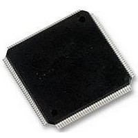
LPC2292FBD144 NXP Semiconductors, LPC2292FBD144 Datasheet - Page 19

LPC2292FBD144
Manufacturer Part Number
LPC2292FBD144
Description
16/32BIT ARM7 MCU, 256K FLASH, 144LQFP
Manufacturer
NXP Semiconductors
Datasheet
1.LPC2292FBD144.pdf
(53 pages)
Specifications of LPC2292FBD144
No. Of I/o's
112
Ram Memory Size
16KB
Cpu Speed
60MHz
No. Of Timers
2
No. Of Pwm Channels
6
Digital Ic Case
RoHS Compliant
Core Size
32bit
Program Memory Size
256KB
Oscillator Type
External Only
Controller Family/series
LPC22xx
Rohs Compliant
Yes
Available stocks
Company
Part Number
Manufacturer
Quantity
Price
Company:
Part Number:
LPC2292FBD144
Manufacturer:
NXP
Quantity:
5 000
Company:
Part Number:
LPC2292FBD144
Manufacturer:
NXP
Quantity:
2
Part Number:
LPC2292FBD144
Manufacturer:
PHILIPS/飞利浦
Quantity:
20 000
Company:
Part Number:
LPC2292FBD144,551
Manufacturer:
NXP Semiconductors
Quantity:
10 000
Part Number:
LPC2292FBD144/00
Manufacturer:
NXP/恩智浦
Quantity:
20 000
Company:
Part Number:
LPC2292FBD144/01
Manufacturer:
NXP
Quantity:
5 000
Company:
Part Number:
LPC2292FBD144/01
Manufacturer:
NXP
Quantity:
2 000
Company:
Part Number:
LPC2292FBD144/01
Manufacturer:
NXP
Quantity:
3
Company:
Part Number:
LPC2292FBD144/01,5
Manufacturer:
NXP Semiconductors
Quantity:
10 000
NXP Semiconductors
LPC2292_2294_7
Product data sheet
6.8.1 Features
6.8.2 Features added with the Fast GPIO set of registers available on
6.9.1 Features
6.9.2 ADC features available in LPC2292/LPC2294/01 only
6.8 General purpose parallel I/O (GPIO) and Fast I/O
6.9 10-bit ADC
Device pins that are not connected to a specific peripheral function are controlled by the
parallel I/O registers. Pins may be dynamically configured as inputs or outputs. Separate
registers allow setting or clearing any number of outputs simultaneously. The value of the
output register may be read back, as well as the current state of the port pins.
LPC2292/LPC2294/01 only
The LPC2292/LPC2294 each contain a single 10-bit successive approximation ADC with
four multiplexed channels.
•
•
•
•
•
•
•
•
•
•
•
•
•
•
•
•
Bit-level set and clear registers allow a single instruction set or clear of any number of
bits in one port.
Direction control of individual bits.
Separate control of output set and clear.
All I/O default to inputs after reset.
Fast GPIO registers are relocated to the ARM local bus for the fastest possible I/O
timing, enabling port pin toggling up to 3.5 times faster than earlier LPC2000 devices.
Mask registers allow treating sets of port bits as a group, leaving other bits
unchanged.
All Fast GPIO registers are byte addressable.
Entire port value can be written in one instruction.
Ports are accessible via either the legacy group of registers (GPIOs) or the group of
registers providing accelerated port access (Fast GPIOs).
Measurement range of 0 V to 3 V.
Capable of performing more than 400000 10-bit samples per second.
Burst conversion mode for single or multiple inputs.
Optional conversion on transition on input pin or Timer Match signal.
Every analog input has a dedicated result register to reduce interrupt overhead.
Every analog input can generate an interrupt once the conversion is completed.
The ADC pads are 5 V tolerant when configured for digital I/O function(s).
Rev. 7 — 4 December 2008
16/32-bit ARM microcontrollers with external memory interface
LPC2292/LPC2294
© NXP B.V. 2008. All rights reserved.
19 of 53


