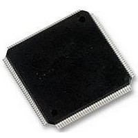
LPC2292FBD144 NXP Semiconductors, LPC2292FBD144 Datasheet - Page 14

LPC2292FBD144
Manufacturer Part Number
LPC2292FBD144
Description
16/32BIT ARM7 MCU, 256K FLASH, 144LQFP
Manufacturer
NXP Semiconductors
Datasheet
1.LPC2292FBD144.pdf
(53 pages)
Specifications of LPC2292FBD144
No. Of I/o's
112
Ram Memory Size
16KB
Cpu Speed
60MHz
No. Of Timers
2
No. Of Pwm Channels
6
Digital Ic Case
RoHS Compliant
Core Size
32bit
Program Memory Size
256KB
Oscillator Type
External Only
Controller Family/series
LPC22xx
Rohs Compliant
Yes
Available stocks
Company
Part Number
Manufacturer
Quantity
Price
Company:
Part Number:
LPC2292FBD144
Manufacturer:
NXP
Quantity:
5 000
Company:
Part Number:
LPC2292FBD144
Manufacturer:
NXP
Quantity:
2
Part Number:
LPC2292FBD144
Manufacturer:
PHILIPS/飞利浦
Quantity:
20 000
Company:
Part Number:
LPC2292FBD144,551
Manufacturer:
NXP Semiconductors
Quantity:
10 000
Part Number:
LPC2292FBD144/00
Manufacturer:
NXP/恩智浦
Quantity:
20 000
Company:
Part Number:
LPC2292FBD144/01
Manufacturer:
NXP
Quantity:
5 000
Company:
Part Number:
LPC2292FBD144/01
Manufacturer:
NXP
Quantity:
2 000
Company:
Part Number:
LPC2292FBD144/01
Manufacturer:
NXP
Quantity:
3
Company:
Part Number:
LPC2292FBD144/01,5
Manufacturer:
NXP Semiconductors
Quantity:
10 000
NXP Semiconductors
Table 4.
[1]
[2]
[3]
[4]
[5]
[6]
[7]
[8]
[9]
LPC2292_2294_7
Product data sheet
Symbol
V
V
V
DDA(1V8)
DD(3V3)
DDA(3V3)
LPC2294 only.
5 V tolerant pad providing digital I/O functions with TTL levels and hysteresis and 10 ns slew rate control.
SSP interface available on LPC2292/2294/01 only.
5 V tolerant pad providing digital I/O functions with TTL levels and hysteresis and 10 ns slew rate control. If configured for an input
function, this pad utilizes built-in glitch filter that blocks pulses shorter than 3 ns.
Open-drain 5 V tolerant digital I/O I
functionality. Open-drain configuration applies to all output functions on this pin.
5 V tolerant pad providing digital I/O (with TTL levels and hysteresis and 10 ns slew rate control) and analog input function. If configured
for a digital input function, this pad utilizes built-in glitch filter that blocks pulses shorter than 3 ns. When configured as an ADC input,
digital section of the pad is disabled.
5 V tolerant pad with built-in pull-up resistor providing digital I/O functions with TTL levels and hysteresis and 10 ns slew rate control.
The pull-up resistor’s value ranges from 60 k to 300 k .
5 V tolerant pad providing digital input (with TTL levels and hysteresis) function only.
Pad provides special analog functionality.
Pin description
Pin (LQFP)
143
2, 31, 39, 51,
57, 77, 94,
104, 112, 119
14
…continued
Pin
(TFBGA)
A2
B1, K3, M3,
M6, N8, K10,
F12, C13,
A11, B9
F3
2
C-bus 400 kHz specification compatible pad. It requires external pull-up to provide an output
[1]
Type
I
I
I
Rev. 7 — 4 December 2008
16/32-bit ARM microcontrollers with external memory interface
Description
Analog 1.8 V core power supply: This is the power supply
voltage for internal circuitry. This should be nominally the
same voltage as V
noise and error.
3.3 V pad power supply: This is the power supply voltage for
the I/O ports.
Analog 3.3 V pad power supply: This should be nominally
the same voltage as V
minimize noise and error.
DD(1V8)
LPC2292/LPC2294
DD(3V3)
but should be isolated to minimize
but should be isolated to
© NXP B.V. 2008. All rights reserved.
14 of 53


