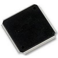
LPC2292FBD144 NXP Semiconductors, LPC2292FBD144 Datasheet - Page 18

LPC2292FBD144
Manufacturer Part Number
LPC2292FBD144
Description
16/32BIT ARM7 MCU, 256K FLASH, 144LQFP
Manufacturer
NXP Semiconductors
Datasheet
1.LPC2292FBD144.pdf
(53 pages)
Specifications of LPC2292FBD144
No. Of I/o's
112
Ram Memory Size
16KB
Cpu Speed
60MHz
No. Of Timers
2
No. Of Pwm Channels
6
Digital Ic Case
RoHS Compliant
Core Size
32bit
Program Memory Size
256KB
Oscillator Type
External Only
Controller Family/series
LPC22xx
Rohs Compliant
Yes
Available stocks
Company
Part Number
Manufacturer
Quantity
Price
Company:
Part Number:
LPC2292FBD144
Manufacturer:
NXP
Quantity:
5 000
Company:
Part Number:
LPC2292FBD144
Manufacturer:
NXP
Quantity:
2
Part Number:
LPC2292FBD144
Manufacturer:
PHILIPS/飞利浦
Quantity:
20 000
Company:
Part Number:
LPC2292FBD144,551
Manufacturer:
NXP Semiconductors
Quantity:
10 000
Part Number:
LPC2292FBD144/00
Manufacturer:
NXP/恩智浦
Quantity:
20 000
Company:
Part Number:
LPC2292FBD144/01
Manufacturer:
NXP
Quantity:
5 000
Company:
Part Number:
LPC2292FBD144/01
Manufacturer:
NXP
Quantity:
2 000
Company:
Part Number:
LPC2292FBD144/01
Manufacturer:
NXP
Quantity:
3
Company:
Part Number:
LPC2292FBD144/01,5
Manufacturer:
NXP Semiconductors
Quantity:
10 000
NXP Semiconductors
LPC2292_2294_7
Product data sheet
6.6 Pin connect block
6.7 External memory controller
Table 5.
[1]
The pin connect block allows selected pins of the microcontroller to have more than one
function. Configuration registers control the multiplexers to allow connection between the
pin and the on chip peripherals. Peripherals should be connected to the appropriate pins
prior to being activated, and prior to any related interrupt(s) being enabled. Activity of any
enabled peripheral function that is not mapped to a related pin should be considered
undefined.
The external Static Memory Controller is a module which provides an interface between
the system bus and external (off-chip) memory devices. It provides support for up to four
independently configurable memory banks (16 MB each with byte lane enable control)
simultaneously. Each memory bank is capable of supporting SRAM, ROM, flash EPROM,
burst ROM memory, or some external I/O devices.
Each memory bank may be 8-bit, 16-bit, or 32-bit wide.
Block
UART1
PWM0
I2C
SPI0
SPI1 and SSP
PLL
RTC
System Control
ADC
CAN
SSP interface and UART0/1 auto-baud control are available on LPC2292/2294/01 only.
Interrupt sources
[1]
Flag(s)
RX Line Status (RLS)
Transmit Holding Register empty (THRE)
RX Data Available (RDA)
Character Time-out Indicator (CTI)
Modem Status Interrupt (MSI)
Auto-baud time-out (ABTO)
End of auto-baud (ABEO)
Match 0 to 6 (MR0, MR1, MR2, MR3, MR4, MR5, MR6)
SI (state change)
SPIF, MODF
SPIF, MODF and TXRIS, RXRIS, RTRIS, RORRIS
PLL Lock (PLOCK)
RTCCIF (Counter Increment), RTCALF (Alarm)
External Interrupt 0 (EINT0)
External Interrupt 1 (EINT1)
External Interrupt 2 (EINT2)
External Interrupt 3 (EINT3)
ADC
1 ORed CAN Acceptance Filter
CAN1/2 Tx
CAN2/3 Tx (LPC2294 only)
reserved
CAN1/2 Rx
CAN3/4 Rx (LPC2294 only)
Rev. 7 — 4 December 2008
16/32-bit ARM microcontrollers with external memory interface
…continued
[1]
[1]
LPC2292/LPC2294
© NXP B.V. 2008. All rights reserved.
VIC channel #
7
8
9
10
11
12
13
14
15
16
17
18
19
20, 21
22, 23
24, 25
26, 27
28,29
18 of 53


