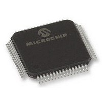
DSPIC30F5011-30I/PTG Microchip Technology, DSPIC30F5011-30I/PTG Datasheet - Page 85

DSPIC30F5011-30I/PTG
Manufacturer Part Number
DSPIC30F5011-30I/PTG
Description
16BIT MCU-DSP 30MHZ, SMD, 30F5011
Manufacturer
Microchip Technology
Series
DsPIC30Fr
Datasheet
1.DSPIC30F5011-30IPTG.pdf
(220 pages)
Specifications of DSPIC30F5011-30I/PTG
Core Frequency
30MHz
Embedded Interface Type
CAN, I2C, SPI, UART
No. Of I/o's
52
Flash Memory Size
66KB
Supply Voltage Range
2.5V To 5.5V
Operating Temperature Range
-40°C To
Lead Free Status / RoHS Status
Lead free / RoHS Compliant
- Current page: 85 of 220
- Download datasheet (4Mb)
13.4.2
The PWM period is specified by writing to the PRx
register. The PWM period can be calculated using
Equation 13-1.
EQUATION 13-1:
PWM frequency is defined as 1 / [PWM period].
FIGURE 13-2:
13.5
When the CPU enters Sleep mode, all internal clocks
are stopped. Therefore, when the CPU enters the
Sleep state, the output compare channel will drive the
pin to the active state that was observed prior to
entering the CPU Sleep state.
For example, if the pin was high when the CPU entered
the Sleep state, the pin will remain high. Likewise, if the
pin was low when the CPU entered the Sleep state, the
pin will remain low. In either case, the output compare
module will resume operation when the device wakes
up.
13.6
When the CPU enters the Idle mode, the output
compare module can operate with full functionality.
The output compare channel will operate during the
CPU Idle mode if the OCSIDL bit (OCxCON<13>) is at
logic ‘0’ and the selected time base (Timer2 or Timer3)
is enabled and the TSIDL bit of the selected timer is set
to logic ‘0’.
2004 Microchip Technology Inc.
PWM period = [(PRx) + 1] • 4 • T
Output Compare Operation During
CPU Sleep Mode
Output Compare Operation During
CPU Idle Mode
PWM PERIOD
OCxR = OCxRS
(Interrupt Flag)
TMR3 = PR3
T3IF = 1
(TMRx prescale value)
PWM OUTPUT TIMING
Duty Cycle
OSC
Period
TMR3 = Duty Cycle
•
(OCxR)
Preliminary
OCxR = OCxRS
(Interrupt Flag)
TMR3 = PR3
T3IF = 1
When the selected TMRx is equal to its respective
period register, PRx, the following four events occur on
the next increment cycle:
• TMRx is cleared.
• The OCx pin is set.
• The PWM duty cycle is latched from OCxRS into
• The corresponding timer interrupt flag is set.
See Figure 13-2 for key PWM period comparisons.
Timer3 is referred to in Figure 13-2 for clarity.
13.7
The output compare channels have the ability to gener-
ate an interrupt on a compare match, for whichever
Match mode has been selected.
For all modes except the PWM mode, when a compare
event occurs, the respective interrupt flag (OCxIF) is
asserted and an interrupt will be generated if enabled.
The OCxIF bit is located in the corresponding IFS
Status register and must be cleared in software. The
interrupt is enabled via the respective compare inter-
rupt enable (OCxIE) bit located in the corresponding
IEC Control register.
For the PWM mode, when an event occurs, the respec-
tive timer interrupt flag (T2IF or T3IF) is asserted and
an interrupt will be generated if enabled. The IF bit is
located in the IFS0 Status register and must be cleared
in software. The interrupt is enabled via the respective
timer interrupt enable bit (T2IE or T3IE) located in the
IEC0 Control register. The output compare interrupt
flag is never set during the PWM mode of operation.
- Exception 1: If PWM duty cycle is 0x0000,
- Exception 2: If duty cycle is greater than PRx,
OCxR.
TMR3 = Duty Cycle
dsPIC30F5011/5013
the OCx pin will remain low.
the pin will remain high.
(OCxR)
Output Compare Interrupts
DS70116C-page 83
Related parts for DSPIC30F5011-30I/PTG
Image
Part Number
Description
Manufacturer
Datasheet
Request
R

Part Number:
Description:
IC DSPIC MCU/DSP 66K 64TQFP
Manufacturer:
Microchip Technology
Datasheet:

Part Number:
Description:
IC,DSP,16-BIT,CMOS,TQFP,64PIN,PLASTIC
Manufacturer:
Microchip Technology
Datasheet:

Part Number:
Description:
IC DSPIC MCU/DSP 66K 64TQFP
Manufacturer:
Microchip Technology
Datasheet:

Part Number:
Description:
High-Performance Digital Signal Controllers
Manufacturer:
MICROCHIP [Microchip Technology]
Datasheet:

Part Number:
Description:
IC, DSC, 16BIT, 66KB, 40MHZ 5.5V TQFP-64
Manufacturer:
Microchip Technology
Datasheet:

Part Number:
Description:
Digital Signal Processors & Controllers - DSP, DSC 16 Bit MCU/DSP 64LD 20M 66KB FL
Manufacturer:
Microchip Technology

Part Number:
Description:
IC DSPIC MCU/DSP 66K 64TQFP
Manufacturer:
Microchip Technology
Datasheet:

Part Number:
Description:
Dspic30f5011/5013 High-performance Digital Signal Controllers
Manufacturer:
Microchip Technology Inc.
Datasheet:

Part Number:
Description:
Manufacturer:
Microchip Technology Inc.
Datasheet:

Part Number:
Description:
Manufacturer:
Microchip Technology Inc.
Datasheet:

Part Number:
Description:
Manufacturer:
Microchip Technology Inc.
Datasheet:

Part Number:
Description:
Manufacturer:
Microchip Technology Inc.
Datasheet:


