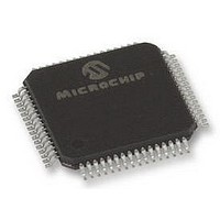
DSPIC30F5011-30I/PTG Microchip Technology, DSPIC30F5011-30I/PTG Datasheet - Page 59

DSPIC30F5011-30I/PTG
Manufacturer Part Number
DSPIC30F5011-30I/PTG
Description
16BIT MCU-DSP 30MHZ, SMD, 30F5011
Manufacturer
Microchip Technology
Series
DsPIC30Fr
Datasheet
1.DSPIC30F5011-30IPTG.pdf
(220 pages)
Specifications of DSPIC30F5011-30I/PTG
Core Frequency
30MHz
Embedded Interface Type
CAN, I2C, SPI, UART
No. Of I/o's
52
Flash Memory Size
66KB
Supply Voltage Range
2.5V To 5.5V
Operating Temperature Range
-40°C To
Lead Free Status / RoHS Status
Lead free / RoHS Compliant
- Current page: 59 of 220
- Download datasheet (4Mb)
8.0
All of the device pins (except V
OSC1/CLKI) are shared between the peripherals and
the parallel I/O ports.
All I/O input ports feature Schmitt Trigger inputs for
improved noise immunity.
8.1
When a peripheral is enabled and the peripheral is
actively driving an associated pin, the use of the pin as
a general purpose output pin is disabled. The I/O pin
may be read but the output driver for the parallel port bit
will be disabled. If a peripheral is enabled but the
peripheral is not actively driving a pin, that pin may be
driven by a port.
All port pins have three registers directly associated
with the operation of the port pin. The Data Direction
register (TRISx) determines whether the pin is an input
or an output. If the data direction bit is a ‘1’, then the pin
is an input. All port pins are defined as inputs after a
Reset. Reads from the latch (LATx), read the latch.
Writes to the latch, write the latch (LATx). Reads from
the port (PORTx), read the port pins and writes to the
port pins, write the latch (LATx).
Any bit and its associated data and control registers
that are not valid for a particular device will be dis-
abled. That means the corresponding LATx and TRISx
registers and the port pin will read as zeros.
FIGURE 8-1:
2004 Microchip Technology Inc.
I/O PORTS
Parallel I/O (PIO) Ports
BLOCK DIAGRAM OF A DEDICATED PORT STRUCTURE
Data Bus
WR TRIS
WR LAT +
WR Port
Read LAT
Read Port
DD
, V
Read TRIS
SS
Dedicated Port Module
, MCLR and
TRIS Latch
Data Latch
D
D
CK
CK
Preliminary
Q
Q
When a pin is shared with another peripheral or func-
tion that is defined as an input only, it is nevertheless
regarded as a dedicated port because there is no
other competing source of outputs. An example is the
INT4 pin.
The format of the registers for PORTA are shown in
Table 8-1.
The TRISA (Data Direction Control) register controls
the direction of the RA<7:0> pins, as well as the INTx
pins and the V
data to the outputs and is readable/writable. Reading
the PORTA register yields the state of the input pins,
while writing the PORTA register modifies the contents
of the LATA register.
A parallel I/O (PIO) port that shares a pin with a periph-
eral is, in general, subservient to the peripheral. The
peripheral’s output buffer data and control signals are
provided to a pair of multiplexers. The multiplexers
select whether the peripheral or the associated port
has ownership of the output data and control signals of
the I/O pad cell. Figure 8-2 shows how ports are shared
with other peripherals and the associated I/O cell (pad)
to which they are connected. Table 8-2 through
Table 8-9 show the formats of the registers for the
shared ports, PORTB through PORTG.
Note:
dsPIC30F5011/5013
The actual bits in use vary between
devices.
REF
I/O Cell
pins. The LATA register supplies
I/O Pad
DS70116C-page 57
Related parts for DSPIC30F5011-30I/PTG
Image
Part Number
Description
Manufacturer
Datasheet
Request
R

Part Number:
Description:
IC DSPIC MCU/DSP 66K 64TQFP
Manufacturer:
Microchip Technology
Datasheet:

Part Number:
Description:
IC,DSP,16-BIT,CMOS,TQFP,64PIN,PLASTIC
Manufacturer:
Microchip Technology
Datasheet:

Part Number:
Description:
IC DSPIC MCU/DSP 66K 64TQFP
Manufacturer:
Microchip Technology
Datasheet:

Part Number:
Description:
High-Performance Digital Signal Controllers
Manufacturer:
MICROCHIP [Microchip Technology]
Datasheet:

Part Number:
Description:
IC, DSC, 16BIT, 66KB, 40MHZ 5.5V TQFP-64
Manufacturer:
Microchip Technology
Datasheet:

Part Number:
Description:
Digital Signal Processors & Controllers - DSP, DSC 16 Bit MCU/DSP 64LD 20M 66KB FL
Manufacturer:
Microchip Technology

Part Number:
Description:
IC DSPIC MCU/DSP 66K 64TQFP
Manufacturer:
Microchip Technology
Datasheet:

Part Number:
Description:
Dspic30f5011/5013 High-performance Digital Signal Controllers
Manufacturer:
Microchip Technology Inc.
Datasheet:

Part Number:
Description:
Manufacturer:
Microchip Technology Inc.
Datasheet:

Part Number:
Description:
Manufacturer:
Microchip Technology Inc.
Datasheet:

Part Number:
Description:
Manufacturer:
Microchip Technology Inc.
Datasheet:

Part Number:
Description:
Manufacturer:
Microchip Technology Inc.
Datasheet:


