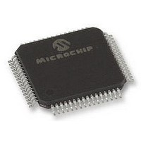
DSPIC30F5011-30I/PTG Microchip Technology, DSPIC30F5011-30I/PTG Datasheet - Page 124

DSPIC30F5011-30I/PTG
Manufacturer Part Number
DSPIC30F5011-30I/PTG
Description
16BIT MCU-DSP 30MHZ, SMD, 30F5011
Manufacturer
Microchip Technology
Series
DsPIC30Fr
Datasheet
1.DSPIC30F5011-30IPTG.pdf
(220 pages)
Specifications of DSPIC30F5011-30I/PTG
Core Frequency
30MHz
Embedded Interface Type
CAN, I2C, SPI, UART
No. Of I/o's
52
Flash Memory Size
66KB
Supply Voltage Range
2.5V To 5.5V
Operating Temperature Range
-40°C To
Lead Free Status / RoHS Status
Lead free / RoHS Compliant
- Current page: 124 of 220
- Download datasheet (4Mb)
dsPIC30F5011/5013
18.3.11
The RSCON SFR contains control bits that are used to
enable up to 16 time slots for reception. These control
bits are the RSE<15:0> bits. The size of each receive
time slot is determined by the WS<3:0> word size
selection bits and can vary from 1 to 16 bits.
If a receive time slot is enabled via one of the RSE bits
(RSEx = 1), the shift register contents will be written to
the current DCI receive shadow buffer location and the
buffer control unit will be incremented to point to the
next buffer location.
Data is not packed in the receive memory buffer loca-
tions if the selected word size is less than 16 bits. Each
received slot data word is stored in a separate 16-bit
buffer location. Data is always stored in a left justified
format in the receive memory buffer.
18.3.12
The TSE and RSE control bits operate in concert with
the DCI frame sync generator. In the Master mode, a
COFS signal is generated whenever the frame sync
generator is reset. In the Slave mode, the frame sync
generator is reset whenever a COFS pulse is received.
The TSE and RSE control bits allow up to 16 consecu-
tive time slots to be enabled for transmit or receive.
After the last enabled time slot has been transmitted/
received, the DCI will stop buffering data until the next
occurring COFS pulse.
18.3.13
The DCI buffer control unit will be incremented by one
word location whenever a given time slot has been
enabled for transmission or reception. In most cases,
data input and output transfers will be synchronized,
which means that a data sample is received for a given
channel at the same time a data sample is transmitted.
Therefore, the transmit and receive buffers will be filled
with equal amounts of data when a DCI interrupt is
generated.
In some cases, the amount of data transmitted and
received during a data frame may not be equal. As an
example, assume a two-word data frame is used. Fur-
thermore, assume that data is only received during
slot #0 but is transmitted during slot #0 and slot #1. In
this case, the buffer control unit counter would be incre-
mented twice during a data frame but only one receive
register location would be filled with data.
DS70116C-page 122
RECEIVE SLOT ENABLE BITS
SLOT ENABLE BITS OPERATION
WITH FRAME SYNC
SYNCHRONOUS DATA
TRANSFERS
Preliminary
18.3.14
The amount of data that is buffered between interrupts
is determined by the buffer length (BLEN<1:0>) control
bits in the DCISTAT SFR. The size of the transmit and
receive buffers may be varied from 1 to 4 data words
using the BLEN control bits. The BLEN control bits are
compared to the current value of the DCI buffer control
unit address counter. When the 2 LS bits of the DCI
address counter match the BLEN<1:0> value, the
buffer control unit will be reset to ‘0’. In addition, the
contents of the receive shadow registers are trans-
ferred to the receive buffer registers and the contents
of the transmit buffer registers are transferred to the
transmit shadow registers.
18.3.15
There is no direct coupling between the position of the
AGU address pointer and the data frame boundaries.
This means that there will be an implied assignment of
each transmit and receive buffer that is a function of the
BLEN control bits and the number of enabled data slots
via the TSE and RSE control bits.
As an example, assume that a 4-word data frame is
chosen and that we want to transmit on all four time
slots in the frame. This configuration would be estab-
lished by setting the TSE0, TSE1, TSE2, and TSE3
control bits in the TSCON SFR. With this module setup,
the TXBUF0 register would be naturally assigned to
slot #0, the TXBUF1 register would be naturally
assigned to slot #1, and so on.
Note:
BUFFER ALIGNMENT WITH DATA
FRAMES
When more than four time slots are active
within a data frame, the user code must
keep track of which time slots are to be
read/written at each interrupt. In some
cases, the alignment between transmit/
receive buffers and their respective slot
assignments could be lost. Examples of
such cases include an emulation break-
point or a hardware trap. In these situa-
tions, the user should poll the SLOT status
bits to determine what data should be
loaded
resynchronize the software with the DCI
module.
BUFFER LENGTH CONTROL
into
2004 Microchip Technology Inc.
the
buffer
registers to
Related parts for DSPIC30F5011-30I/PTG
Image
Part Number
Description
Manufacturer
Datasheet
Request
R

Part Number:
Description:
IC DSPIC MCU/DSP 66K 64TQFP
Manufacturer:
Microchip Technology
Datasheet:

Part Number:
Description:
IC,DSP,16-BIT,CMOS,TQFP,64PIN,PLASTIC
Manufacturer:
Microchip Technology
Datasheet:

Part Number:
Description:
IC DSPIC MCU/DSP 66K 64TQFP
Manufacturer:
Microchip Technology
Datasheet:

Part Number:
Description:
High-Performance Digital Signal Controllers
Manufacturer:
MICROCHIP [Microchip Technology]
Datasheet:

Part Number:
Description:
IC, DSC, 16BIT, 66KB, 40MHZ 5.5V TQFP-64
Manufacturer:
Microchip Technology
Datasheet:

Part Number:
Description:
Digital Signal Processors & Controllers - DSP, DSC 16 Bit MCU/DSP 64LD 20M 66KB FL
Manufacturer:
Microchip Technology

Part Number:
Description:
IC DSPIC MCU/DSP 66K 64TQFP
Manufacturer:
Microchip Technology
Datasheet:

Part Number:
Description:
Dspic30f5011/5013 High-performance Digital Signal Controllers
Manufacturer:
Microchip Technology Inc.
Datasheet:

Part Number:
Description:
Manufacturer:
Microchip Technology Inc.
Datasheet:

Part Number:
Description:
Manufacturer:
Microchip Technology Inc.
Datasheet:

Part Number:
Description:
Manufacturer:
Microchip Technology Inc.
Datasheet:

Part Number:
Description:
Manufacturer:
Microchip Technology Inc.
Datasheet:


