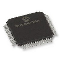
DSPIC30F5011-30I/PTG Microchip Technology, DSPIC30F5011-30I/PTG Datasheet - Page 41

DSPIC30F5011-30I/PTG
Manufacturer Part Number
DSPIC30F5011-30I/PTG
Description
16BIT MCU-DSP 30MHZ, SMD, 30F5011
Manufacturer
Microchip Technology
Series
DsPIC30Fr
Datasheet
1.DSPIC30F5011-30IPTG.pdf
(220 pages)
Specifications of DSPIC30F5011-30I/PTG
Core Frequency
30MHz
Embedded Interface Type
CAN, I2C, SPI, UART
No. Of I/o's
52
Flash Memory Size
66KB
Supply Voltage Range
2.5V To 5.5V
Operating Temperature Range
-40°C To
Lead Free Status / RoHS Status
Lead free / RoHS Compliant
- Current page: 41 of 220
- Download datasheet (4Mb)
5.0
The dsPIC30F Sensor and General Purpose Family
has up to 41 interrupt sources and 4 processor excep-
tions (traps) which must be arbitrated based on a
priority scheme.
The CPU is responsible for reading the Interrupt Vector
Table (IVT) and transferring the address contained in
the interrupt vector to the program counter. The inter-
rupt vector is transferred from the program data bus
into the program counter via a 24-bit wide multiplexer
on the input of the program counter.
The Interrupt Vector Table (IVT) and Alternate Interrupt
Vector Table (AIVT) are placed near the beginning of
program memory (0x000004). The IVT and AIVT are
shown in Figure 5-1.
The interrupt controller is responsible for pre-
processing the interrupts and processor exceptions
prior to them being presented to the processor core.
The peripheral interrupts and traps are enabled, priori-
tized and controlled using centralized Special Function
Registers:
• IFS0<15:0>, IFS1<15:0>, IFS2<15:0>
• IEC0<15:0>, IEC1<15:0>, IEC2<15:0>
• IPC0<15:0>... IPC10<7:0>
• IPL<3:0>
• INTCON1<15:0>, INTCON2<15:0>
2004 Microchip Technology Inc.
All interrupt request flags are maintained in these
three registers. The flags are set by their respec-
tive peripherals or external signals, and they are
cleared via software.
All interrupt enable control bits are maintained in
these three registers. These control bits are used
to individually enable interrupts from the
peripherals or external signals.
The user assignable priority level associated with
each of these 41 interrupts is held centrally in
these twelve registers.
The current CPU priority level is explicitly stored
in the IPL bits. IPL<3> is present in the CORCON
register, whereas IPL<2:0> are present in the
STATUS register (SR) in the processor core.
Global interrupt control functions are derived from
these two registers. INTCON1 contains the con-
trol and status flags for the processor exceptions.
The INTCON2 register controls the external
interrupt request signal behavior and the use of
the alternate vector table.
Note:
INTERRUPTS
Interrupt flag bits get set when an interrupt
condition occurs, regardless of the state of
its corresponding enable bit. User soft-
ware should ensure the appropriate inter-
rupt flag bits are clear prior to enabling an
interrupt.
Preliminary
All interrupt sources can be user assigned to one of 7
priority levels, 1 through 7, via the IPCx registers. Each
interrupt source is associated with an interrupt vector,
as shown in Table 5-1. Levels 7 and 1 represent the
highest and lowest maskable priorities, respectively.
If the NSTDIS bit (INTCON1<15>) is set, nesting of
interrupts is prevented. Thus, if an interrupt is currently
being serviced, processing of a new interrupt is pre-
vented even if the new interrupt is of higher priority than
the one currently being serviced.
Certain interrupts have specialized control bits for fea-
tures like edge or level triggered interrupts, interrupt-
on-change, etc. Control of these features remains
within the peripheral module which generates the
interrupt.
The DISI instruction can be used to disable the
processing of interrupts of priorities 6 and lower for a
certain number of instructions, during which the DISI bit
(INTCON2<14>) remains set.
When an interrupt is serviced, the PC is loaded with the
address stored in the vector location in program mem-
ory that corresponds to the interrupt. There are 63 dif-
ferent vectors within the IVT (refer to Table 5-1). These
vectors are contained in locations 0x000004 through
0x0000FE of program memory (refer to Table 5-1).
These locations contain 24-bit addresses and in order
to preserve robustness, an address error trap will take
place should the PC attempt to fetch any of these
words during normal execution. This prevents execu-
tion of random data as a result of accidentally decre-
menting a PC into vector space, accidentally mapping
a data space address into vector space, or the PC roll-
ing over to 0x000000 after reaching the end of imple-
mented program memory space. Execution of a GOTO
instruction to this vector space will also generate an
address error trap.
Note:
Note:
dsPIC30F5011/5013
Assigning a priority level of ‘0’ to an inter-
rupt source is equivalent to disabling that
interrupt.
The IPL bits become read only whenever
the NSTDIS bit has been set to ‘1’.
DS70116C-page 39
Related parts for DSPIC30F5011-30I/PTG
Image
Part Number
Description
Manufacturer
Datasheet
Request
R

Part Number:
Description:
IC DSPIC MCU/DSP 66K 64TQFP
Manufacturer:
Microchip Technology
Datasheet:

Part Number:
Description:
IC,DSP,16-BIT,CMOS,TQFP,64PIN,PLASTIC
Manufacturer:
Microchip Technology
Datasheet:

Part Number:
Description:
IC DSPIC MCU/DSP 66K 64TQFP
Manufacturer:
Microchip Technology
Datasheet:

Part Number:
Description:
High-Performance Digital Signal Controllers
Manufacturer:
MICROCHIP [Microchip Technology]
Datasheet:

Part Number:
Description:
IC, DSC, 16BIT, 66KB, 40MHZ 5.5V TQFP-64
Manufacturer:
Microchip Technology
Datasheet:

Part Number:
Description:
Digital Signal Processors & Controllers - DSP, DSC 16 Bit MCU/DSP 64LD 20M 66KB FL
Manufacturer:
Microchip Technology

Part Number:
Description:
IC DSPIC MCU/DSP 66K 64TQFP
Manufacturer:
Microchip Technology
Datasheet:

Part Number:
Description:
Dspic30f5011/5013 High-performance Digital Signal Controllers
Manufacturer:
Microchip Technology Inc.
Datasheet:

Part Number:
Description:
Manufacturer:
Microchip Technology Inc.
Datasheet:

Part Number:
Description:
Manufacturer:
Microchip Technology Inc.
Datasheet:

Part Number:
Description:
Manufacturer:
Microchip Technology Inc.
Datasheet:

Part Number:
Description:
Manufacturer:
Microchip Technology Inc.
Datasheet:


