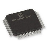
DSPIC30F5011-30I/PTG Microchip Technology, DSPIC30F5011-30I/PTG Datasheet - Page 145

DSPIC30F5011-30I/PTG
Manufacturer Part Number
DSPIC30F5011-30I/PTG
Description
16BIT MCU-DSP 30MHZ, SMD, 30F5011
Manufacturer
Microchip Technology
Series
DsPIC30Fr
Datasheet
1.DSPIC30F5011-30IPTG.pdf
(220 pages)
Specifications of DSPIC30F5011-30I/PTG
Core Frequency
30MHz
Embedded Interface Type
CAN, I2C, SPI, UART
No. Of I/o's
52
Flash Memory Size
66KB
Supply Voltage Range
2.5V To 5.5V
Operating Temperature Range
-40°C To
Lead Free Status / RoHS Status
Lead free / RoHS Compliant
- Current page: 145 of 220
- Download datasheet (4Mb)
20.3.1.1
The oscillator start-up circuitry is not linked to the POR
circuitry. Some crystal circuits (especially low fre-
quency crystals) will have a relatively long start-up
time. Therefore, one or more of the following conditions
is possible after the POR timer and the PWRT have
expired:
• The oscillator circuit has not begun to oscillate.
• The Oscillator Start-up Timer has not expired (if a
• The PLL has not achieved a LOCK (if PLL is
If the FSCM is enabled and one of the above conditions
is true, then a clock failure trap will occur. The device
will automatically switch to the FRC oscillator and the
user can switch to the desired crystal oscillator in the
trap ISR.
20.3.1.2
If the FSCM is disabled and the Power-up Timer
(PWRT) is also disabled, then the device will exit rap-
idly from Reset on power-up. If the clock source is
FRC, LPRC, EXTRC or EC, it will be active
immediately.
If the FSCM is disabled and the system clock has not
started, the device will be in a frozen state at the Reset
vector until the system clock starts. From the user’s
perspective, the device will appear to be in Reset until
a system clock is available.
20.3.2
The BOR (Brown-out Reset) module is based on an
internal voltage reference circuit. The main purpose of
the BOR module is to generate a device Reset when a
brown-out condition occurs. Brown-out conditions are
generally caused by glitches on the AC mains (i.e.,
missing portions of the AC cycle waveform due to bad
power transmission lines, or voltage sags due to exces-
sive current draw when a large inductive load is turned
on).
The BOR module allows selection of one of the
following voltage trip points:
• 2.0V
• 2.7V
• 4.2V
• 4.5V
2004 Microchip Technology Inc.
crystal oscillator is used).
used).
Note:
BOR: PROGRAMMABLE
BROWN-OUT RESET
The BOR voltage trip points indicated here
are nominal values provided for design
guidance only. Refer to the Electrical
Specifications in the specific device data
sheet for BOR voltage limit specifications.
POR with Long Crystal Start-up Time
(with FSCM Enabled)
Operating without FSCM and PWRT
Preliminary
A BOR will generate a Reset pulse which will reset the
device. The BOR will select the clock source based on
the device configuration bit values (FOS<1:0> and
FPR<3:0>). Furthermore, if an Oscillator mode is
selected, the BOR will activate the Oscillator Start-up
Timer (OST). The system clock is held until OST
expires. If the PLL is used, then the clock will be held
until the LOCK bit (OSCCON<5>) is ‘1’.
Concurrently, the POR time-out (T
time-out (T
is released. If T
used, then a nominal delay of T
The total delay in this case is (T
The BOR status bit (RCON<1>) will be set to indicate
that a BOR has occurred. The BOR circuit, if enabled,
will continue to operate while in Sleep or Idle modes
and will reset the device should V
threshold voltage.
FIGURE 20-6:
Note 1:
Note:
dsPIC30F5011/5013
2:
3:
PWRT
Dedicated supervisory devices, such as
the MCP1XX and MCP8XX, may also be
used as an external Power-on Reset
circuit.
D
External Power-on Reset circuit is required
only if the V
The diode D helps discharge the capacitor
quickly when V
R should be suitably chosen so as to make
sure that the voltage drop across R does not
violate the device’s electrical specifications.
R1 should be suitably chosen so as to limit
any current flowing into MCLR from external
capacitor C, in the event of MCLR/V
breakdown due to Electrostatic Discharge
(ESD), or Electrical Overstress (EOS).
PWRT
) will be applied before the internal Reset
V
DD
R
C
= 0 and a crystal oscillator is being
EXTERNAL POWER-ON
RESET CIRCUIT (FOR
SLOW V
DD
power-up slope is too slow.
DD
R1
powers down.
FSCM
POR
DD
DD
POR
+ T
DS70116C-page 143
dsPIC30F
= 100 s is applied.
MCLR
fall below the BOR
POWER-UP)
) and the PWRT
FSCM
).
PP
pin
Related parts for DSPIC30F5011-30I/PTG
Image
Part Number
Description
Manufacturer
Datasheet
Request
R

Part Number:
Description:
IC DSPIC MCU/DSP 66K 64TQFP
Manufacturer:
Microchip Technology
Datasheet:

Part Number:
Description:
IC,DSP,16-BIT,CMOS,TQFP,64PIN,PLASTIC
Manufacturer:
Microchip Technology
Datasheet:

Part Number:
Description:
IC DSPIC MCU/DSP 66K 64TQFP
Manufacturer:
Microchip Technology
Datasheet:

Part Number:
Description:
High-Performance Digital Signal Controllers
Manufacturer:
MICROCHIP [Microchip Technology]
Datasheet:

Part Number:
Description:
IC, DSC, 16BIT, 66KB, 40MHZ 5.5V TQFP-64
Manufacturer:
Microchip Technology
Datasheet:

Part Number:
Description:
Digital Signal Processors & Controllers - DSP, DSC 16 Bit MCU/DSP 64LD 20M 66KB FL
Manufacturer:
Microchip Technology

Part Number:
Description:
IC DSPIC MCU/DSP 66K 64TQFP
Manufacturer:
Microchip Technology
Datasheet:

Part Number:
Description:
Dspic30f5011/5013 High-performance Digital Signal Controllers
Manufacturer:
Microchip Technology Inc.
Datasheet:

Part Number:
Description:
Manufacturer:
Microchip Technology Inc.
Datasheet:

Part Number:
Description:
Manufacturer:
Microchip Technology Inc.
Datasheet:

Part Number:
Description:
Manufacturer:
Microchip Technology Inc.
Datasheet:

Part Number:
Description:
Manufacturer:
Microchip Technology Inc.
Datasheet:


