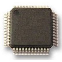
DP83848VYB National Semiconductor, DP83848VYB Datasheet - Page 9

DP83848VYB
Manufacturer Part Number
DP83848VYB
Description
TRANSCEIVER, ENET PHY, 10/100, 48LQFP
Manufacturer
National Semiconductor
Datasheet
1.DP83848VYB.pdf
(76 pages)
Specifications of DP83848VYB
Data Rate
100Mbps
No. Of Ports
1
Ethernet Type
IEEE 802.3u
Supply Current
92mA
Supply Voltage Range
3V To 3.6V
Operating Temperature Range
-40°C To +105°C
Digital Ic Case Style
LQFP
No.
RoHS Compliant
Interface Type
MII Serial, RMII
Rohs Compliant
Yes
Lead Free Status / Rohs Status
Not Compliant
Available stocks
Company
Part Number
Manufacturer
Quantity
Price
Company:
Part Number:
DP83848VYB/NOPB
Manufacturer:
NS
Quantity:
570
Company:
Part Number:
DP83848VYB/NOPB
Manufacturer:
Texas Instruments
Quantity:
10 000
LED_LINK
LED_SPEED
LED_ACT/COL
TCK
TDI
TDO
TMS
TRST#
RESET_N
PWR_DOWN/INT
1.4 LED INTERFACE
See Table 3 for LED Mode Selection.
1.5 JTAG INTERFACE
1.6 RESET AND POWER DOWN
Signal Name
Signal Name
Signal Name
S, O, PU
S, O, PU
S, O, PU
Type
I, PU
I, PU
Type
Type
I, PU
I, PU
I, PU
I, PU
O
Pin #
Pin #
29
Pin #
7
28
27
26
12
10
11
8
9
RESET: Active Low input that initializes or re-initializes the DP83848VYB.
Asserting this pin low for at least 1 µs will force a reset process to occur. All internal
registers will re-initialize to their default states as specified for each bit in the
Register Block section. All strap options are re-initialized as well.
See Section 5.5 POWER DOWN/INTERRUPT for detailed description.
The default function of this pin is POWER DOWN.
POWER DOWN: The pin is an active low input in this mode and should be
asserted low to put the device in a Power Down mode.
INTERRUPT: The pin is an open drain output in this mode and will be asserted
low when an interrupt condition occurs. Although the pin has a weak internal pull-
up, some applications may require an external pull-up resister. Register access
is required for the pin to be used as an interrupt mechanism. See Section 5.5.2
Interrupt Mechanisms for more details on the interrupt mechanisms.
LINK LED: In Mode 1, this pin indicates the status of the LINK. The LED will be
ON when Link is good.
LINK/ACT LED: In Mode 2 and Mode 3, this pin indicates transmit and receive
activity in addition to the status of the Link. The LED will be ON when Link is
good. It will blink when the transmitter or receiver is active.
SPEED LED: The LED is ON when device is in 100 Mb/s and OFF when in 10
Mb/s. Functionality of this LED is independent of mode selected.
ACTIVITY LED: In Mode 1, this pin is the Activity LED which is ON when activity
is present on either Transmit or Receive.
COLLISION/DUPLEX LED: In Mode 2, this pin by default indicates Collision
detection. For Mode 3, this LED output may be programmed to indicate Full-
duplex status instead of Collision.
TEST CLOCK
This pin has a weak internal pullup.
TEST DATA INPUT
This pin has a weak internal pullup.
TEST OUTPUT
TEST MODE SELECT
This pin has a weak internal pullup.
TEST RESET: Active low asynchronous test reset.
This pin has a weak internal pullup.
9
Description
Description
Description
www.national.com


