NCP5393MNR2G ON Semiconductor, NCP5393MNR2G Datasheet - Page 6
NCP5393MNR2G
Manufacturer Part Number
NCP5393MNR2G
Description
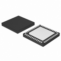
IC CTLR 2/3/4PHASE CPU 48-QFN
Manufacturer
ON Semiconductor
Datasheet
1.NCP5393MNR2G.pdf
(23 pages)
Specifications of NCP5393MNR2G
Applications
Multiphase Controller
Current - Supply
25mA
Voltage - Supply
4.75 V ~ 5.25 V
Operating Temperature
0°C ~ 70°C
Mounting Type
Surface Mount
Package / Case
48-TQFN Exposed Pad
Mounting Style
SMD/SMT
Lead Free Status / RoHS Status
Lead free / RoHS Compliant
Available stocks
Company
Part Number
Manufacturer
Quantity
Price
Company:

Part Number:
NCP5393MNR2G
Manufacturer:
RFMD
Quantity:
10 000
Part Number:
NCP5393MNR2G
Manufacturer:
ON
Quantity:
20 000


NCP5393 PIN DESCRIPTIONS
PIN CONNECTIONS VS. PHASE COUNT
Pin No.
Number of
FLAG
Phases
32
33
34
35
36
37
38
39
40
41
42
43
44
45
46
47
48
4
3
2
NB_DROOP
NB_DRVON
PWRGOOD
NB_COMP
VID3/SVC
VID2/SVD
ENABLE
PWROK
Symbol
DRVON
NB_FB
Phase 4
PGND
NB_G
VID0
VID1
Tie to
Tie to
GND
GND
G4
G3
G2
G1
Out
G4
Phase 3
Phase 3
Phase 2
Voltage output signal proportional to total current drawn from the VDDNB regulator. Used when load
line operation (“droop”) is desired.
Voltage error amplifier inverting input for the V
Output of the voltage error amplifier for the V
Parallel Voltage ID DAC Input 0. Not used in SVI mode.
Parallel Voltage ID DAC Input 1. Also used for PVI or SVI mode selection.
System power supplies status input. Used in SVI mode only.
High = Run, Low = Standby/Reset.
Parallel Voltage ID DAC Input 1. Also used in SVI mode.
Parallel Voltage ID DAC Input 1. Also used in SVI mode.
Open drain output. High indicates that the active output(s) are within specification. Internally pulled
high by 5 mA to V
Bidirectional Gate Drive Enable to the gate driver for the V
Bidirectional Gate Drive Enable to gate drivers for the V
PWM output to the V
PWM output #4. See Table: “Pin Connections vs. Phase Count”
PWM output #3. See Table: “Pin Connections vs. Phase Count”
PWM output #2. See Table: “Pin Connections vs. Phase Count”
PWM output #1. See Table: “Pin Connections vs. Phase Count”
High-current power supply return via metal pad (flag) underneath package. The package flag should
be tied directly to Pin 2.
Out
Out
Out
G3
Phase 2
Phase 2
Tie to
GND
Out
Out
G2
CC
DDNB
http://onsemi.com
Phase 1
Phase 1
Phase 1
gate driver.
Out
Out
Out
G1
NCP5393
6
Tie to GND/VDD P hase 3 CS
Tie to GND/VDD
Phase 4 CS
CS4 &
CS4N
Input
Description
DDNB
DDNB
regulator.
regulator.
Phase 3 CS
Phase 2 CS
DD
CS3 &
CS3N
DDNB
Input
Input
input
regulator.
regulator.
Tie to GND/VDD Phase 1 CS
Phase 2 CS
Phase 2 CS
CS2 &
CS2N
Input
Input
Phase 1 CS
Phase 1 CS
CS1 &
CS1N
Input
Input
Input
Related parts for NCP5393MNR2G
Image
Part Number
Description
Manufacturer
Datasheet
Request
R

Part Number:
Description:
2/3/4-Phase Controller
Manufacturer:
ON Semiconductor
Datasheet:
Part Number:
Description:
ON Semiconductor [VOLTAGE REGULATOR]
Manufacturer:
ON Semiconductor
Datasheet:
Part Number:
Description:
357-036-542-201 CARDEDGE 36POS DL .156 BLK LOPRO
Manufacturer:
ON Semiconductor
Datasheet:
Part Number:
Description:
357-036-542-201 CARDEDGE 36POS DL .156 BLK LOPRO
Manufacturer:
ON Semiconductor
Datasheet:
Part Number:
Description:
357-036-542-201 CARDEDGE 36POS DL .156 BLK LOPRO
Manufacturer:
ON Semiconductor
Datasheet:
Part Number:
Description:
357-036-542-201 CARDEDGE 36POS DL .156 BLK LOPRO
Manufacturer:
ON Semiconductor
Datasheet:
Part Number:
Description:
357-036-542-201 CARDEDGE 36POS DL .156 BLK LOPRO
Manufacturer:
ON Semiconductor
Datasheet:
Part Number:
Description:
357-036-542-201 CARDEDGE 36POS DL .156 BLK LOPRO
Manufacturer:
ON Semiconductor
Datasheet:
Part Number:
Description:
357-036-542-201 CARDEDGE 36POS DL .156 BLK LOPRO
Manufacturer:
ON Semiconductor
Datasheet:
Part Number:
Description:
357-036-542-201 CARDEDGE 36POS DL .156 BLK LOPRO
Manufacturer:
ON Semiconductor
Datasheet:
Part Number:
Description:
357-036-542-201 CARDEDGE 36POS DL .156 BLK LOPRO
Manufacturer:
ON Semiconductor
Datasheet:
Part Number:
Description:
357-036-542-201 CARDEDGE 36POS DL .156 BLK LOPRO
Manufacturer:
ON Semiconductor
Datasheet:
Part Number:
Description:
Manufacturer:
ON Semiconductor
Datasheet:
Part Number:
Description:
Manufacturer:
ON Semiconductor
Datasheet: