NCP5393MNR2G ON Semiconductor, NCP5393MNR2G Datasheet - Page 5
NCP5393MNR2G
Manufacturer Part Number
NCP5393MNR2G
Description
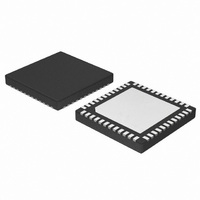
IC CTLR 2/3/4PHASE CPU 48-QFN
Manufacturer
ON Semiconductor
Datasheet
1.NCP5393MNR2G.pdf
(23 pages)
Specifications of NCP5393MNR2G
Applications
Multiphase Controller
Current - Supply
25mA
Voltage - Supply
4.75 V ~ 5.25 V
Operating Temperature
0°C ~ 70°C
Mounting Type
Surface Mount
Package / Case
48-TQFN Exposed Pad
Mounting Style
SMD/SMT
Lead Free Status / RoHS Status
Lead free / RoHS Compliant
Available stocks
Company
Part Number
Manufacturer
Quantity
Price
Company:

Part Number:
NCP5393MNR2G
Manufacturer:
RFMD
Quantity:
10 000
Part Number:
NCP5393MNR2G
Manufacturer:
ON
Quantity:
20 000


NCP5393 PIN DESCRIPTIONS
Pin No.
10
11
12
13
14
15
16
17
18
19
20
21
22
23
24
25
26
27
28
29
30
31
1
2
3
4
5
6
7
8
9
NB_DIFFOUT
NB_OFFSET
DIFFOUT
12VMON
OFFSET
NB_CSN
NB_VS-
NB_VS+
DROOP
Symbol
NB_CS
COMP
VCCA
VCCB
ROSC
PSI_L
CS1N
CS2N
CS3N
CS4N
GND
VFIX
VID4
VID5
VS+
VS-
CS1
CS2
CS3
CS4
ILIM
FB
5 V supply pin for the NCP5393. The V
pin and GND (preferably returned to the package flag).
Small-signal power supply return. This pin should be tied directly to the package flag (exposed pad).
Output of the voltage error amplifier for the V
Voltage error amplifier inverting input for the V
Voltage output signal proportional to total current drawn from the V
operation (“droop”) is desired.
Non-inverting input to the differential remote sense amplifier for the V
Inverting input to the differential remote sense amplifier for the V
Input for offset voltage to be added to the V
offset.
Output of the differential remote sense amplifier for the V
When pulled low, this pin causes the levels on the SVC (VID3) and SVD (VID2) pins to be decoded
as a two-bit DAC code, which controls the V
V
UVLO monitor input for the 12 V power rail.
Power Saving Control. Low = single phase operation, High = normal operation. This pin is not used in
SVI mode.
Non-inverting input to current sense amplifier #1 for the V
vs. Phase Count”
Inverting input to current sense amplifier #1 for the V
Phase Count”
Non-inverting input to current sense amplifier #2 for the V
vs. Phase Count”
Inverting input to current sense amplifier #2 for the V
Phase Count”
Non-inverting input to current sense amplifier #3 for the V
vs. Phase Count”
Inverting input to current sense amplifier #3 for the V
Phase Count”
Non-inverting input to current sense amplifier #4 for the V
vs. Phase Count”
Inverting input to current sense amplifier #4 for the V
Phase Count”
Overcurrent shutdown threshold for V
ally used to develop an appropriate voltage on ILIM.
5 V supply pin. Tie this pin to VCCA (Pin 1).
Non-inverting input to the current sense amplifier for the VDDNB regulator
Inverting input to the current sense amplifier for the VDDNB regulator
Parallel Voltage ID DAC Input 4. Not used in SVI mode.
Parallel Voltage ID DAC Input 5. Not used in SVI mode.
A resistance from this pin to ground programs the V
supplies a trimmed output voltage of 2 V.
Output of the differential remote sense amplifier for the VDDNB regulator.
Input for offset voltage to be added to the VDDNB DAC's output voltage. Ground this pin for zero
VDDNB offset.
Inverting input to the differential remote sense amplifier for the VDDNB regulator.
Non-inverting input to the differential remote sense amplifier for the VDDNB regulator.
CC
http://onsemi.com
NCP5393
5
DD
CC
and VDDNB. A resistor divider from ROSC to GND is typic‐
bypassing capacitance must be connected between this
DD
Description
DD
DD
DD
DAC's output voltage. Ground this pin for zero V
and VDDNB outputs. Internally pulled high by 5 mA to
regulator.
regulator.
DD
DD
DD
DD
DD
and VDDNB oscillator frequencies. This pin
regulator. See Table: “Pin Connections vs.
regulator. See Table: “Pin Connections vs.
regulator. See Table: “Pin Connections vs.
regulator. See Table: “Pin Connections vs.
DD
DD
DD
DD
DD
regulator.
regulator. See Table: “Pin Connections
regulator. See Table: “Pin Connections
regulator. See Table: “Pin Connections
regulator. See Table: “Pin Connections
DD
DD
regulator.
DD
regulator. Used when load line
regulator.
DD
Related parts for NCP5393MNR2G
Image
Part Number
Description
Manufacturer
Datasheet
Request
R

Part Number:
Description:
2/3/4-Phase Controller
Manufacturer:
ON Semiconductor
Datasheet:
Part Number:
Description:
ON Semiconductor [VOLTAGE REGULATOR]
Manufacturer:
ON Semiconductor
Datasheet:
Part Number:
Description:
357-036-542-201 CARDEDGE 36POS DL .156 BLK LOPRO
Manufacturer:
ON Semiconductor
Datasheet:
Part Number:
Description:
357-036-542-201 CARDEDGE 36POS DL .156 BLK LOPRO
Manufacturer:
ON Semiconductor
Datasheet:
Part Number:
Description:
357-036-542-201 CARDEDGE 36POS DL .156 BLK LOPRO
Manufacturer:
ON Semiconductor
Datasheet:
Part Number:
Description:
357-036-542-201 CARDEDGE 36POS DL .156 BLK LOPRO
Manufacturer:
ON Semiconductor
Datasheet:
Part Number:
Description:
357-036-542-201 CARDEDGE 36POS DL .156 BLK LOPRO
Manufacturer:
ON Semiconductor
Datasheet:
Part Number:
Description:
357-036-542-201 CARDEDGE 36POS DL .156 BLK LOPRO
Manufacturer:
ON Semiconductor
Datasheet:
Part Number:
Description:
357-036-542-201 CARDEDGE 36POS DL .156 BLK LOPRO
Manufacturer:
ON Semiconductor
Datasheet:
Part Number:
Description:
357-036-542-201 CARDEDGE 36POS DL .156 BLK LOPRO
Manufacturer:
ON Semiconductor
Datasheet:
Part Number:
Description:
357-036-542-201 CARDEDGE 36POS DL .156 BLK LOPRO
Manufacturer:
ON Semiconductor
Datasheet:
Part Number:
Description:
357-036-542-201 CARDEDGE 36POS DL .156 BLK LOPRO
Manufacturer:
ON Semiconductor
Datasheet:
Part Number:
Description:
Manufacturer:
ON Semiconductor
Datasheet:
Part Number:
Description:
Manufacturer:
ON Semiconductor
Datasheet: