NCP5393MNR2G ON Semiconductor, NCP5393MNR2G Datasheet - Page 13
NCP5393MNR2G
Manufacturer Part Number
NCP5393MNR2G
Description
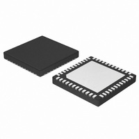
IC CTLR 2/3/4PHASE CPU 48-QFN
Manufacturer
ON Semiconductor
Datasheet
1.NCP5393MNR2G.pdf
(23 pages)
Specifications of NCP5393MNR2G
Applications
Multiphase Controller
Current - Supply
25mA
Voltage - Supply
4.75 V ~ 5.25 V
Operating Temperature
0°C ~ 70°C
Mounting Type
Surface Mount
Package / Case
48-TQFN Exposed Pad
Mounting Style
SMD/SMT
Lead Free Status / RoHS Status
Lead free / RoHS Compliant
Available stocks
Company
Part Number
Manufacturer
Quantity
Price
Company:

Part Number:
NCP5393MNR2G
Manufacturer:
RFMD
Quantity:
10 000
Part Number:
NCP5393MNR2G
Manufacturer:
ON
Quantity:
20 000


Functional Description
General
compatible with both Parallel VID interface (PVI) and
Serial VID interface (SVI) protocols for AMD Processors.
The Controller implements a single-phase control
architecture to provide the Northbridge (NB) voltage on the
same chip. For the CORE section, programmable 2- to-4
phase featuring Dual-Edge multiphase architecture is
implemented. It embeds two independent controllers for
CPU CORE and the integrated NB, each one with its set of
protections.
differential phase current sensing, optional load-line
voltage positioning, and programmable V
offsets to provide accurately regulated power parallel- and
serial-VID AMD processors. Dual-edge multiphase
modulation provides the fastest initial response to dynamic
load events.
testing. In this particular configuration the SVI bus is used
as a static bus configuring four operative voltages (through
SVC and SVD) for both the sections and ignoring any
serial-VID command.
And configures itself to work as a Single-Plane PVI
controller or Dual-Plane SVI controller. The NCP5393
manages On the Fly VID transitions and maintains the slew
rates as defined when the transitions take place. NCP5393
is available in TQFN48 Package.
Remote Output Sensing Amplifier (RSA)
V
reference point by connecting the V
and the V
configuration keeps ground potential differences between the
local controller ground and the V
from affecting regulation of V
ground reference points. The RSA also subtracts the DAC
(minus VID offset) voltage, thereby producing an unamplified
output error voltage at the DIFFOUT pin. This output also has
a 1.3 V bias voltage as the floating ground to allow both
positive and negative error voltages.
Precision Programmable DAC
trimmed. This DAC has 0.5% accuracy over the entire
operating temperature range of the part. The DAC can be
programmed to support both PVI and SVI VID code
specifications.
High Performance Voltage Error Amplifier
and bandwidth. Although not required when operating as the
core
NCP5393 is a universal CPU hybrid power Controller
The NCP5393 incorporates differential voltage sensing,
NCP5393 also supports V_FIX mode for board debug and
NCP5393 is able to detect which kind of CPU is connected
A true differential amplifier allows the NCP5393 to measure
A precision programmable DAC is provided and system
The error amplifier is designed to provide high slew rate
voltage feedback with respect to the V
core
ground reference point to VSN. This
core
core
core
between V
ground reference point
reference point to VSP,
DD
core
and V
core
and V
ground
http://onsemi.com
DDNB
core
NCP5393
13
controller of a voltage regulator, a capacitor from COMP to
VFB is required for stable unity gain test configurations.
Gate Driver Outputs and 2/3/4 Phase Operation
mode. In 2-phase mode, phases 1 and 3 should be used to
drive the external gate drivers, G2 and G4 must be grounded.
In 3-phase mode, gate output G4 must be grounded. In
4-phase mode all 4 gate outputs are used as shown in the
4-phase Applications Schematic. The Current Sense inputs
of unused channels should be connected to GND. Please
refer to table “PIN CONNECTIONS vs. PHASE COUNTS”
for details.
Differential Current Sense Amplifiers and Summing
Amplifier
output current of each phase. The inputs of each current
sense amplifier must be connected across the current sensing
element of the phase controlled by the corresponding gate
output (G1, G2, G3, or G4). If a phase is unused, the
differential inputs to that phase's current sense amplifier
must be shorted together and connected to the GND.
a summing amplifier to have a summed-up output. The
outputs of current sense amplifiers control three functions.
First, the summing current signal of all phases will go
through DROOP amplifier and join the voltage feedback
loop for output voltage positioning. Second, the output
signal from DROOP amplifier also goes to ILIM amplifier
to monitor the output current limit. Finally, the individual
phase current contributes to the current balance of all phases
by offsetting their ramp signals of PWM comparators.
Oscillator and Triangle Wave Generator
dual-Oscillator: one section is used for the CORE and it is
a multiphase programmable oscillator managing equal
phase-shift among all phases and the other section is used
for the NB section. The oscillator's frequency is
programmed by the resistance connected from the ROSC
pin to ground. The user will usually form this resistance
from two resistors in order to create a voltage divider that
uses the ROSC output voltage as the reference for creating
the current limit setpoint voltage. The oscillator frequency
range is 100 kHz per phase to 1.0 MHz per phase. The
oscillator generates up to 4 symmetrical triangle waveforms
with amplitude between 1.3 V and 2.3 V. The triangle waves
have a phase delay between them such that for 2-, 3- and
4-phase operation the PWM outputs are separated by 180,
120, and 90 angular degrees, respectively.
VDDNB oscillator does not accidentally lock to the VDD
The part can be configured to run in 2-, 3-, or 4-phase
Four differential amplifiers are provided to sense the
The current signals sensed from inductor DCR are fed into
The controller embeds a programmable precision
When the NB phase is enabled, in order to ensure that the
Related parts for NCP5393MNR2G
Image
Part Number
Description
Manufacturer
Datasheet
Request
R

Part Number:
Description:
2/3/4-Phase Controller
Manufacturer:
ON Semiconductor
Datasheet:
Part Number:
Description:
ON Semiconductor [VOLTAGE REGULATOR]
Manufacturer:
ON Semiconductor
Datasheet:
Part Number:
Description:
357-036-542-201 CARDEDGE 36POS DL .156 BLK LOPRO
Manufacturer:
ON Semiconductor
Datasheet:
Part Number:
Description:
357-036-542-201 CARDEDGE 36POS DL .156 BLK LOPRO
Manufacturer:
ON Semiconductor
Datasheet:
Part Number:
Description:
357-036-542-201 CARDEDGE 36POS DL .156 BLK LOPRO
Manufacturer:
ON Semiconductor
Datasheet:
Part Number:
Description:
357-036-542-201 CARDEDGE 36POS DL .156 BLK LOPRO
Manufacturer:
ON Semiconductor
Datasheet:
Part Number:
Description:
357-036-542-201 CARDEDGE 36POS DL .156 BLK LOPRO
Manufacturer:
ON Semiconductor
Datasheet:
Part Number:
Description:
357-036-542-201 CARDEDGE 36POS DL .156 BLK LOPRO
Manufacturer:
ON Semiconductor
Datasheet:
Part Number:
Description:
357-036-542-201 CARDEDGE 36POS DL .156 BLK LOPRO
Manufacturer:
ON Semiconductor
Datasheet:
Part Number:
Description:
357-036-542-201 CARDEDGE 36POS DL .156 BLK LOPRO
Manufacturer:
ON Semiconductor
Datasheet:
Part Number:
Description:
357-036-542-201 CARDEDGE 36POS DL .156 BLK LOPRO
Manufacturer:
ON Semiconductor
Datasheet:
Part Number:
Description:
357-036-542-201 CARDEDGE 36POS DL .156 BLK LOPRO
Manufacturer:
ON Semiconductor
Datasheet:
Part Number:
Description:
Manufacturer:
ON Semiconductor
Datasheet:
Part Number:
Description:
Manufacturer:
ON Semiconductor
Datasheet: