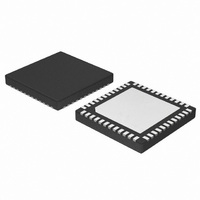
NCP5393MNR2G ON Semiconductor, NCP5393MNR2G Datasheet - Page 21

NCP5393MNR2G
Manufacturer Part Number
NCP5393MNR2G
Description
IC CTLR 2/3/4PHASE CPU 48-QFN
Manufacturer
ON Semiconductor
Datasheet
1.NCP5393MNR2G.pdf
(23 pages)
Specifications of NCP5393MNR2G
Applications
Multiphase Controller
Current - Supply
25mA
Voltage - Supply
4.75 V ~ 5.25 V
Operating Temperature
0°C ~ 70°C
Mounting Type
Surface Mount
Package / Case
48-TQFN Exposed Pad
Mounting Style
SMD/SMT
Lead Free Status / RoHS Status
Lead free / RoHS Compliant
Available stocks
Company
Part Number
Manufacturer
Quantity
Price
Company:
Part Number:
NCP5393MNR2G
Manufacturer:
RFMD
Quantity:
10 000
Part Number:
NCP5393MNR2G
Manufacturer:
ON
Quantity:
20 000
OUTPUT OFFSET VOLTAGES
External offset voltages from 0 mv to 800 mV `above the DAC' can be added for the V
Offset is set by a resistor divider from V
factors change by the same amount:
For example: For 0 V offset: pin voltage = GND; For 800 mV offset: pin voltage = V
The input to the OFFSET pin for the VDD output is encoded by an internal ADC.
The input to the NB_OFFSET pin for the VDDNB output is encoded by the same ADC.
The reference for this ADC is VCC. The ADC's output is ratiometric to VCC.
Voffset IN represents the voltage applied to the OFFSET or NB_OFFSET pin.
It is intended that these voltages be derived by a resistive divider from Vcc.
The recommended total driving impedance is <10 kilohms.
Minimum Voffset_IN
(as Vin/Vcc)
0.046875
0.078125
0.109375
0.140625
0.171875
0.203125
0.234375
0.265625
0.296875
0.328125
0.359375
0.390625
0.421875
0.453125
0.484375
0.515625
0.546875
0.578125
0.609375
0.640625
0.671875
0.703125
0.734375
0.765625
0.796875
0.828125
0.859375
0.890625
0.921875
0.953125
0.984375
0
Typical Voffset_IN
(as Vin/Vcc)
0.06250
0.09375
0.12500
0.15625
0.18750
0.21875
0.25000
0.28125
0.31250
0.34375
0.37500
0.40625
0.43750
0.46875
0.50000
0.53125
0.56250
0.59375
0.62500
0.65625
0.68750
0.71875
0.75000
0.78125
0.81250
0.84375
0.87500
0.90625
0.93750
0.96875
1.00000
CC
0
to GND. Output offsets are ratiometric to V
Offset = 0.8 V x V
http://onsemi.com
NCP5393
Maximum Voffset_IN
21
(as Vin/Vcc)
Vcc+0.3V
0.046875
0.078125
0.109375
0.140625
0.171875
0.203125
0.234375
0.265625
0.296875
0.328125
0.359375
0.390625
0.421875
0.453125
0.484375
0.515625
0.546875
0.578125
0.609375
0.640625
0.671875
0.703125
0.734375
0.765625
0.796875
0.828125
0.859375
0.890625
0.921875
0.953125
0.984375
OFFSET
/V
CC
Resulting Output Offset
CC
CC
. As V
DD
and V
CC
100
125
150
175
200
225
250
275
300
325
350
375
400
425
450
475
500
525
550
575
600
625
650
675
700
725
750
800
25
50
75
0
changes, the on-chip scaling
DD_NB
independently.
Units
mV
mV
mV
mV
mV
mV
mV
mV
mV
mV
mV
mV
mV
mV
mV
mV
mV
mV
mV
mV
mV
mV
mV
mV
mV
mV
mV
mV
mV
mV
mV
mV


