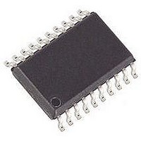
PIC16F721-I/SO Microchip Technology, PIC16F721-I/SO Datasheet - Page 50

PIC16F721-I/SO
Manufacturer Part Number
PIC16F721-I/SO
Description
MCU PIC 4K FLASH 20-SOIC
Manufacturer
Microchip Technology
Series
PIC® XLP™ 16Fr
Datasheets
1.PIC16F722-ISS.pdf
(8 pages)
2.PIC16LF720-ISS.pdf
(244 pages)
3.PIC16F720-ISO.pdf
(36 pages)
4.PIC16F720-ISO.pdf
(8 pages)
5.PIC16F721-IML.pdf
(6 pages)
Specifications of PIC16F721-I/SO
Core Size
8-Bit
Program Memory Size
7KB (4K x 14)
Peripherals
Brown-out Detect/Reset, POR, PWM, WDT
Core Processor
PIC
Speed
16MHz
Connectivity
I²C, SPI, UART/USART
Number Of I /o
17
Program Memory Type
FLASH
Ram Size
256 x 8
Voltage - Supply (vcc/vdd)
1.8 V ~ 5.5 V
Data Converters
A/D 12x8b
Oscillator Type
Internal
Operating Temperature
-40°C ~ 85°C
Package / Case
20-SOIC (0.300", 7.50mm Width)
Controller Family/series
PIC16F
No. Of I/o's
18
Ram Memory Size
256Byte
Cpu Speed
16MHz
No. Of Timers
3
Lead Free Status / RoHS Status
Lead free / RoHS Compliant
Eeprom Size
-
Lead Free Status / RoHS Status
Lead free / RoHS Compliant
- PIC16F722-ISS PDF datasheet
- PIC16LF720-ISS PDF datasheet #2
- PIC16F720-ISO PDF datasheet #3
- PIC16F720-ISO PDF datasheet #4
- PIC16F721-IML PDF datasheet #5
- Current page: 50 of 244
- Download datasheet (3Mb)
PIC16F/LF720/721
6.1.4
Each PORTA pin is multiplexed with other functions. The
pins and their combined functions are briefly described
here. For specific information about individual functions
such as the A/D Converter (ADC), refer to the
appropriate section in this data sheet.
6.1.4.1
Figure 6-1
configurable to function as one of the following:
• a general purpose I/O
• an analog input for the ADC
• ICSP programming data (separate controls from
• ICD Debugging data (separate controls from
6.1.4.2
Figure 6-2
configurable to function as one of the following:
• a general purpose I/O
• an analog input for the ADC
• ICSP programming clock (separate controls from
• ICD Debugging clock (separate controls from
DS41430A-page 50
TRISA)
TRISA)
TRISA)
TRISA)
shows the diagram for this pin. This pin is
shows the diagram for this pin. This pin is
PIN DESCRIPTIONS AND
DIAGRAMS
RA0/AN0/ICSPDAT
RA1/AN1/ICSPCLK
6.1.4.3
Figure 6-3
configurable to function as one of the following:
• a general purpose I/O
• an analog input for the ADC
• external interrupt
• clock input for Timer0
The Timer0 clock input function works independently of
any TRIS register setting. Effectively, if TRISA2 = 0,
the PORTA2 register bit will output to the pad and Clock
Timer0 at the same time.
6.1.4.4
Figure 6-4
configurable to function as one of the following:
• a general purpose I/O
• Master Clear Reset with weak pull-up
6.1.4.5
Figure 6-5
configurable to function as one of the following:
• a general purpose I/O
• analog input for the ADC
• Timer1 gate input
• clock output
6.1.4.6
Figure 6-6
configurable to function as one of the following:
• a general purpose I/O
• Timer1 Clock input
• clock input
shows the diagram for this pin. This pin is
shows the diagram for this pin. This pin is
shows the diagram for this pin. This pin is
shows the diagram for this pin. This pin is
RA2/AN2/T0CKI/INT
RA3/MCLR/V
RA4/AN3/T1G/CLKOUT
RA5/T1CKI/CLKIN
2010 Microchip Technology Inc.
PP
Related parts for PIC16F721-I/SO
Image
Part Number
Description
Manufacturer
Datasheet
Request
R

Part Number:
Description:
MCU PIC 4K FLASH 20-SSOP
Manufacturer:
Microchip Technology
Datasheet:

Part Number:
Description:
MCU PIC 4K FLASH 20-QFN
Manufacturer:
Microchip Technology
Datasheet:

Part Number:
Description:
MCU PIC 4K FLASH 20-DIP
Manufacturer:
Microchip Technology
Datasheet:

Part Number:
Description:
7 KB FLASH, 256 B SRAM, 18 I/O 20 QFN 4x4mm TUBE
Manufacturer:
Microchip Technology
Datasheet:

Part Number:
Description:
7 KB FLASH, 256 B SRAM, 18 I/O 20 PDIP .300in TUBE
Manufacturer:
Microchip Technology
Datasheet:

Part Number:
Description:
7 KB FLASH, 256 B SRAM, 18 I/O 20 SOIC .300in TUBE
Manufacturer:
Microchip Technology
Datasheet:

Part Number:
Description:
7 KB FLASH, 256 B SRAM, 18 I/O 20 SSOP .209in TUBE
Manufacturer:
Microchip Technology
Datasheet:

Part Number:
Description:
IC PIC MCU FLASH 2KX14 28-QFN
Manufacturer:
Microchip Technology
Datasheet:

Part Number:
Description:
IC PIC MCU FLASH 2KX14 28-SOIC
Manufacturer:
Microchip Technology
Datasheet:

Part Number:
Description:
IC PIC MCU FLASH 2KX14 28DIP
Manufacturer:
Microchip Technology
Datasheet:

Part Number:
Description:
IC PIC MCU FLASH 2KX14 28-SOIC
Manufacturer:
Microchip Technology
Datasheet:

Part Number:
Description:
IC PIC MCU FLASH 2KX14 28QFN
Manufacturer:
Microchip Technology

Part Number:
Description:
IC PIC MCU FLASH 2KX14 28SSOP
Manufacturer:
Microchip Technology

Part Number:
Description:
IC PIC MCU FLASH 2KX14 8-SSOP
Manufacturer:
Microchip Technology
Datasheet:

Part Number:
Description:
IC PIC MCU FLASH 2KX14 28-SSOP
Manufacturer:
Microchip Technology
Datasheet:


