PIC16F721-I/SO Microchip Technology, PIC16F721-I/SO Datasheet - Page 145
PIC16F721-I/SO
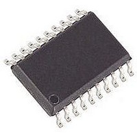
Manufacturer Part Number
PIC16F721-I/SO
Description
MCU PIC 4K FLASH 20-SOIC
Manufacturer
Microchip Technology
Series
PIC® XLP™ 16Fr
Datasheets
1.PIC16F722-ISS.pdf
(8 pages)
2.PIC16LF720-ISS.pdf
(244 pages)
3.PIC16F720-ISO.pdf
(36 pages)
4.PIC16F720-ISO.pdf
(8 pages)
5.PIC16F721-IML.pdf
(6 pages)
Specifications of PIC16F721-I/SO
Core Size
8-Bit
Program Memory Size
7KB (4K x 14)
Peripherals
Brown-out Detect/Reset, POR, PWM, WDT
Core Processor
PIC
Speed
16MHz
Connectivity
I²C, SPI, UART/USART
Number Of I /o
17
Program Memory Type
FLASH
Ram Size
256 x 8
Voltage - Supply (vcc/vdd)
1.8 V ~ 5.5 V
Data Converters
A/D 12x8b
Oscillator Type
Internal
Operating Temperature
-40°C ~ 85°C
Package / Case
20-SOIC (0.300", 7.50mm Width)
Controller Family/series
PIC16F
No. Of I/o's
18
Ram Memory Size
256Byte
Cpu Speed
16MHz
No. Of Timers
3
Lead Free Status / RoHS Status
Lead free / RoHS Compliant
Eeprom Size
-
Lead Free Status / RoHS Status
Lead free / RoHS Compliant


17.1.2.4
The SS pin allows Synchronous Slave mode operation.
The SPI must be in Slave mode with SS pin control
enabled (SSPM<3:0> = 0100). The associated TRIS bit
for the SS pin must be set, making SS an input.
In Slave Select mode, when:
• SS = 0, The device operates as specified in
• SS = 1, The SPI module is held in Reset and the
FIGURE 17-6:
2010 Microchip Technology Inc.
SS
SCK
(CKP = 0
CKE = 0)
SCK
(CKP = 1
CKE = 0)
Write to
SSPBUF
SDO
SDI
(SMP = 0)
Input
Sample
(SMP = 0)
SSPIF
Interrupt
Flag
SSPSR to
SSPBUF
Section 17.1.2 “Slave
SDO pin will be tri-stated.
Note 1: When the SPI is in Slave mode with SS
2: If the SPI is used in Slave mode with CKE
pin control enabled (SSPM<3:0> = 0100),
the SPI module will reset if the SS pin is
driven high.
set, the SS pin control must be enabled.
Slave Select Operation
SLAVE SELECT SYNCHRONIZATION WAVEFORM
Mode”.
bit 7
bit 7
bit 6
When the SPI module resets, the bit counter is cleared
to ‘0’. This can be done by either forcing the SS pin to
a high level or clearing the SSPEN bit.
shows the timing waveform for such a synchronization
event.
17.1.2.5
While in Sleep mode, the slave can transmit/receive
data. The SPI Transmit/Receive Shift register operates
asynchronously to the device on the externally supplied
clock source. This allows the device to be placed in
Sleep mode and data to be shifted into the SPI Trans-
mit/Receive Shift register. When all 8 bits have been
received, the SSP Interrupt Flag bit will be set and, if
enabled, will wake the device from Sleep.
Note:
PIC16F/LF720/721
SSPSR must be reinitialized by writing to
the SSPBUF register before the data can
be clocked out of the slave again.
SSPSR must be reinitialized by writing to
the SSPBUF register before the data can
be clocked out of the slave again.
Sleep in Slave Mode
bit 7
bit 7
DS41430A-page 145
bit 0
bit 0
Figure 17-6
Related parts for PIC16F721-I/SO
Image
Part Number
Description
Manufacturer
Datasheet
Request
R

Part Number:
Description:
MCU PIC 4K FLASH 20-SSOP
Manufacturer:
Microchip Technology
Datasheet:

Part Number:
Description:
MCU PIC 4K FLASH 20-QFN
Manufacturer:
Microchip Technology
Datasheet:

Part Number:
Description:
MCU PIC 4K FLASH 20-DIP
Manufacturer:
Microchip Technology
Datasheet:

Part Number:
Description:
7 KB FLASH, 256 B SRAM, 18 I/O 20 QFN 4x4mm TUBE
Manufacturer:
Microchip Technology
Datasheet:
Part Number:
Description:
7 KB FLASH, 256 B SRAM, 18 I/O 20 PDIP .300in TUBE
Manufacturer:
Microchip Technology
Datasheet:
Part Number:
Description:
7 KB FLASH, 256 B SRAM, 18 I/O 20 SOIC .300in TUBE
Manufacturer:
Microchip Technology
Datasheet:
Part Number:
Description:
7 KB FLASH, 256 B SRAM, 18 I/O 20 SSOP .209in TUBE
Manufacturer:
Microchip Technology
Datasheet:

Part Number:
Description:
IC PIC MCU FLASH 2KX14 28-QFN
Manufacturer:
Microchip Technology
Datasheet:

Part Number:
Description:
IC PIC MCU FLASH 2KX14 28-SOIC
Manufacturer:
Microchip Technology
Datasheet:

Part Number:
Description:
IC PIC MCU FLASH 2KX14 28DIP
Manufacturer:
Microchip Technology
Datasheet:
Part Number:
Description:
IC PIC MCU FLASH 2KX14 28-SOIC
Manufacturer:
Microchip Technology
Datasheet:
Part Number:
Description:
IC PIC MCU FLASH 2KX14 28QFN
Manufacturer:
Microchip Technology

Part Number:
Description:
IC PIC MCU FLASH 2KX14 28SSOP
Manufacturer:
Microchip Technology
Part Number:
Description:
IC PIC MCU FLASH 2KX14 8-SSOP
Manufacturer:
Microchip Technology
Datasheet:
Part Number:
Description:
IC PIC MCU FLASH 2KX14 28-SSOP
Manufacturer:
Microchip Technology
Datasheet: