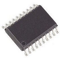
PIC16F721-I/SO Microchip Technology, PIC16F721-I/SO Datasheet - Page 162

PIC16F721-I/SO
Manufacturer Part Number
PIC16F721-I/SO
Description
MCU PIC 4K FLASH 20-SOIC
Manufacturer
Microchip Technology
Series
PIC® XLP™ 16Fr
Datasheets
1.PIC16F722-ISS.pdf
(8 pages)
2.PIC16LF720-ISS.pdf
(244 pages)
3.PIC16F720-ISO.pdf
(36 pages)
4.PIC16F720-ISO.pdf
(8 pages)
5.PIC16F721-IML.pdf
(6 pages)
Specifications of PIC16F721-I/SO
Core Size
8-Bit
Program Memory Size
7KB (4K x 14)
Peripherals
Brown-out Detect/Reset, POR, PWM, WDT
Core Processor
PIC
Speed
16MHz
Connectivity
I²C, SPI, UART/USART
Number Of I /o
17
Program Memory Type
FLASH
Ram Size
256 x 8
Voltage - Supply (vcc/vdd)
1.8 V ~ 5.5 V
Data Converters
A/D 12x8b
Oscillator Type
Internal
Operating Temperature
-40°C ~ 85°C
Package / Case
20-SOIC (0.300", 7.50mm Width)
Controller Family/series
PIC16F
No. Of I/o's
18
Ram Memory Size
256Byte
Cpu Speed
16MHz
No. Of Timers
3
Lead Free Status / RoHS Status
Lead free / RoHS Compliant
Eeprom Size
-
Lead Free Status / RoHS Status
Lead free / RoHS Compliant
- PIC16F722-ISS PDF datasheet
- PIC16LF720-ISS PDF datasheet #2
- PIC16F720-ISO PDF datasheet #3
- PIC16F720-ISO PDF datasheet #4
- PIC16F721-IML PDF datasheet #5
- Current page: 162 of 244
- Download datasheet (3Mb)
PIC16F/LF720/721
FIGURE 18-1:
18.2
When the device is code-protected, the CPU may
continue to read and write the Flash program memory.
Depending on the settings of the Flash program
memory enable (WRT<1:0>) bits, the device may or
may not be able to write certain blocks of the program
memory. However, reads of the program memory are
allowed.
When the Flash program memory Code Protection
(CP) bit in the Configuration Word register is enabled,
the program memory is code-protected, and the device
programmer (ICSP™) cannot access data or program
memory.
18.3
The PMADRH:PMADRL register pair can address up
to a maximum of 4K words of program Flash. The Most
Significant Byte (MSB) of the address is written to the
PMADRH register and the Least Significant Byte (LSB)
is written to the PMADRL register.
DS41430A-page 162
Note:
Flash ADDR
Flash DATA
PMDATH
PMDATL
Register
RD bit
Code Protection
PMADRH and PMADRL Registers
Force
NOP
Stop
PC
Code-protect does not affect the CPU
from performing a read operation on the
program memory. For more information,
refer to Section 8.2 “Code Protection”.
Q1 Q2 Q3 Q4 Q1 Q2 Q3 Q4 Q1 Q2 Q3 Q4 Q1 Q2 Q3 Q4 Q1 Q2 Q3 Q4 Q1 Q2 Q3 Q4
INSTR (PC - 1)
Executed here
PC
FLASH PROGRAM MEMORY READ CYCLE EXECUTION – NORMAL MODE
INSTR (PC)
BSF PMCON1, RD
Executed here
PC + 1
INSTR (PC + 1)
PMADRH, PMADRL
Executed here
Forced NOP
PMDATH, PMDATL
18.4
PMCON1 is the control register for the data program
memory accesses.
Control bits RD and WR initiate read and write,
respectively. These bits cannot be cleared, but only set
in software. They are cleared in hardware at the
completion of the read or write operation. The inability
to clear the WR bit in software prevents the accidental
premature termination of a write operation. Setting the
control bit WR initiates a write operation. For program
memory writes, WR initiates a write cycle if FREE = 0
and an erase cycle if FREE = 1.
The WREN bit, when set, will allow a write operation.
On power-up, the WREN bit is clear. PMCON2 is not a
physical register. Reading PMCON2 will read all ‘0’s.
The PMCON2 register is used exclusively in the Flash
memory write sequence.
Executed here
Forced NOP
PC+3
PMCON1 and PMCON2 Registers
INSTR (PC + 3)
INSTR (PC + 3)
Executed here
2010 Microchip Technology Inc.
PC + 4
INSTR (PC + 4)
INSTR (PC + 4)
Executed here
PC + 5
Related parts for PIC16F721-I/SO
Image
Part Number
Description
Manufacturer
Datasheet
Request
R

Part Number:
Description:
MCU PIC 4K FLASH 20-SSOP
Manufacturer:
Microchip Technology
Datasheet:

Part Number:
Description:
MCU PIC 4K FLASH 20-QFN
Manufacturer:
Microchip Technology
Datasheet:

Part Number:
Description:
MCU PIC 4K FLASH 20-DIP
Manufacturer:
Microchip Technology
Datasheet:

Part Number:
Description:
7 KB FLASH, 256 B SRAM, 18 I/O 20 QFN 4x4mm TUBE
Manufacturer:
Microchip Technology
Datasheet:

Part Number:
Description:
7 KB FLASH, 256 B SRAM, 18 I/O 20 PDIP .300in TUBE
Manufacturer:
Microchip Technology
Datasheet:

Part Number:
Description:
7 KB FLASH, 256 B SRAM, 18 I/O 20 SOIC .300in TUBE
Manufacturer:
Microchip Technology
Datasheet:

Part Number:
Description:
7 KB FLASH, 256 B SRAM, 18 I/O 20 SSOP .209in TUBE
Manufacturer:
Microchip Technology
Datasheet:

Part Number:
Description:
IC PIC MCU FLASH 2KX14 28-QFN
Manufacturer:
Microchip Technology
Datasheet:

Part Number:
Description:
IC PIC MCU FLASH 2KX14 28-SOIC
Manufacturer:
Microchip Technology
Datasheet:

Part Number:
Description:
IC PIC MCU FLASH 2KX14 28DIP
Manufacturer:
Microchip Technology
Datasheet:

Part Number:
Description:
IC PIC MCU FLASH 2KX14 28-SOIC
Manufacturer:
Microchip Technology
Datasheet:

Part Number:
Description:
IC PIC MCU FLASH 2KX14 28QFN
Manufacturer:
Microchip Technology

Part Number:
Description:
IC PIC MCU FLASH 2KX14 28SSOP
Manufacturer:
Microchip Technology

Part Number:
Description:
IC PIC MCU FLASH 2KX14 8-SSOP
Manufacturer:
Microchip Technology
Datasheet:

Part Number:
Description:
IC PIC MCU FLASH 2KX14 28-SSOP
Manufacturer:
Microchip Technology
Datasheet:


