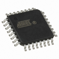
ATMEGA32M1-AUR Atmel, ATMEGA32M1-AUR Datasheet - Page 72

ATMEGA32M1-AUR
Manufacturer Part Number
ATMEGA32M1-AUR
Description
IC MPU AVR 32K 20MHZ 32TQFP
Manufacturer
Atmel
Series
AVR® ATmegar
Specifications of ATMEGA32M1-AUR
Core Processor
AVR
Core Size
8-Bit
Speed
16MHz
Connectivity
CAN, LIN, SPI, UART/USART
Peripherals
Brown-out Detect/Reset, POR, PWM, Temp Sensor, WDT
Program Memory Size
32KB (16K x 16)
Program Memory Type
FLASH
Eeprom Size
1K x 8
Ram Size
2K x 8
Voltage - Supply (vcc/vdd)
2.7 V ~ 5.5 V
Data Converters
A/D 11x10b; D/A 1x10b
Oscillator Type
Internal
Operating Temperature
-40°C ~ 85°C
Package / Case
32-TQFP
Lead Free Status / RoHS Status
Lead free / RoHS Compliant
Number Of I /o
-
Available stocks
Company
Part Number
Manufacturer
Quantity
Price
- Current page: 72 of 341
- Download datasheet (6Mb)
• ADC6/INT2/ACMPN1/AMP2-/PCINT5 – Bit 5
ADC6, Analog to Digital Converter, input channel 6.
INT2, External Interrupt source 2. This pin can serve as an External Interrupt source to the MCU.
ACMPN1, Analog Comparator 1 Negative Input. Configure the port pin as input with the internal
pull-up switched off to avoid the digital port function from interfering with the function of the Ana-
log Comparator.
PCINT5, Pin Change Interrupt 5.
• APM0+/PCINT4 – Bit 4
AMP0+, Analog Differential Amplifier 0 Positive Input Channel.
PCINT4, Pin Change Interrupt 4.
• AMP0-/PCINT3 – Bit 3
AMP0-, Analog Differential Amplifier 0 Negative Input Channel. Configure the port pin as input
with the internal pull-up switched off to avoid the digital port function from interfering with the
function of the Analog Amplifier.
PCINT3, Pin Change Interrupt 3.
• ADC5/INT1/ACMPN0/PCINT2 – Bit 2
ADC5, Analog to Digital Converter, input channel 5.
INT1, External Interrupt source 1. This pin can serve as an external interrupt source to the MCU.
ACMPN0, Analog Comparator 0 Negative Input. Configure the port pin as input with the internal
pull-up switched off to avoid the digital port function from interfering with the function of the Ana-
log Comparator.
PCINT2, Pin Change Interrupt 2.
• PCINT1/MOSI/PSCOUT2B – Bit 1
MOSI: SPI Master Data output, Slave Data input for SPI channel. When the SPI is enabled as a
slave, this pin is configured as an input regardless of the setting of DDB1 When the SPI is
enabled as a master, the data direction of this pin is controlled by DDB1. When the pin is forced
to be an input, the pull-up can still be controlled by the PORTB1 and PUD bits.
PSCOUT2B, Output 2B of PSC.
PCINT1, Pin Change Interrupt 1.
• PCINT0/MISO/PSCOUT2A – Bit 0
MISO, Master Data input, Slave Data output pin for SPI channel. When the SPI is enabled as a
master, this pin is configured as an input regardless of the setting of DDB0. When the SPI is
enabled as a slave, the data direction of this pin is controlled by DDB0. When the pin is forced to
be an input, the pull-up can still be controlled by the PORTB0 and PUD bits.
PSCOUT2A, Output 2A of PSC.
PCINT0, Pin Change Interrupt 0.
ATmega16M1/32M1/64M1
72
8209D–AVR–11/10
Related parts for ATMEGA32M1-AUR
Image
Part Number
Description
Manufacturer
Datasheet
Request
R

Part Number:
Description:
Manufacturer:
Atmel Corporation
Datasheet:

Part Number:
Description:
Manufacturer:
ATMEL Corporation
Datasheet:

Part Number:
Description:
IC AVR MCU 32K 16MHZ 5V 44-QFN
Manufacturer:
Atmel
Datasheet:

Part Number:
Description:
IC AVR MCU 32K 16MHZ 5V 40DIP
Manufacturer:
Atmel
Datasheet:

Part Number:
Description:
IC AVR MCU 32K 16MHZ 5V 44TQFP
Manufacturer:
Atmel
Datasheet:

Part Number:
Description:
IC AVR MCU 32K 16MHZ IND 40-DIP
Manufacturer:
Atmel
Datasheet:

Part Number:
Description:
IC AVR MCU 32K 16MHZ IND 44-TQFP
Manufacturer:
Atmel
Datasheet:

Part Number:
Description:
MCU AVR 32KB FLASH 16MHZ 44TQFP
Manufacturer:
Atmel
Datasheet:

Part Number:
Description:
MCU AVR 32KB FLASH 16MHZ 44QFN
Manufacturer:
Atmel
Datasheet:

Part Number:
Description:
MCU AVR 32K FLASH 16MHZ 44-TQFP
Manufacturer:
Atmel
Datasheet:

Part Number:
Description:
IC AVR MCU 32K 16MHZ COM 40-DIP
Manufacturer:
Atmel
Datasheet:

Part Number:
Description:
IC AVR MCU 32K 16MHZ COM 44-QFN
Manufacturer:
Atmel
Datasheet:

Part Number:
Description:
IC AVR MCU 32K 16MHZ COM 44-TQFP
Manufacturer:
Atmel
Datasheet:


