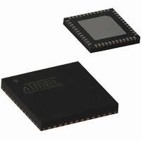
ATA5428-PLQW Atmel, ATA5428-PLQW Datasheet - Page 92

ATA5428-PLQW
Manufacturer Part Number
ATA5428-PLQW
Description
IC TXRX WIDEBND 433/868MHZ 48QFN
Manufacturer
Atmel
Specifications of ATA5428-PLQW
Frequency
433MHz, 868MHz
Data Rate - Maximum
20kbps
Modulation Or Protocol
ASK, FSK
Applications
Alarm and Security Systems, RKE
Power - Output
10dBm
Sensitivity
-112.5dBm
Voltage - Supply
2.4 V ~ 3.6 V or 4.4 V ~ 6.6 V
Current - Receiving
10.5mA
Current - Transmitting
10mA
Data Interface
PCB, Surface Mount
Antenna Connector
PCB, Surface Mount
Operating Temperature
-40°C ~ 85°C
Package / Case
48-VQFN Exposed Pad, 48-HVQFN, 48-SQFN, 48-DHVQFN
Operating Temperature (min)
-40C
Operating Temperature (max)
85C
Operating Temperature Classification
Industrial
Product Depth (mm)
7mm
Product Height (mm)
0.9mm
Product Length (mm)
7mm
Lead Free Status / RoHS Status
Lead free / RoHS Compliant
Memory Size
-
Lead Free Status / Rohs Status
Compliant
Other names
ATA5428-PLQHCT
ATA5428-PLQHCT
ATA5428-PLQWCT
ATA5428-PLQHCT
ATA5428-PLQWCT
Available stocks
Company
Part Number
Manufacturer
Quantity
Price
Company:
Part Number:
ATA5428-PLQW
Manufacturer:
LITELINK
Quantity:
106
Part Number:
ATA5428-PLQW
Manufacturer:
ATMEL/爱特梅尔
Quantity:
20 000
16. Digital Timing Characteristics (Continued)
All parameters refer to GND and are valid for T
application (6V)) and V
92
*) Type means: A = 100% tested, B = 100% correlation tested, C = Characterized on samples, D = Design parameter
15.10
15.11
13.6
13.7
14.1
15.1
15.2
15.3
15.4
15.5
15.6
15.7
15.8
15.9
No.
14
15
Parameters
Minimum time period
between edges at pin
SDO_TMDO in RX
transparent mode
Edge
period of the data signal
for full sensitivity in RX
mode
TX Mode
Start
Configuration of the Transceiver with 4-wire Serial Interface
CS set
edge of SCK
SCK cycle time
SDI_TMDI set
to rising edge of SCK
SDI_TMDI hold time
from rising edge of SCK
SDO_TMDO enable
time from rising edge of
CS
SDO_TMDO output
delay from falling edge
of SCK
SDO_TMDO disable
time from falling edge of
CS
CS disable time period
Time period SCK low to
CS high
Time period SCK low to
CS low
Time period CS low to
SCK high
ATA5423/ATA5425/ATA5428/ATA5429
-
-
up time
to
-
up time to rising
-
edge time
VS2
-
up time
= 5.0V (Base
Test Conditions
XLIM = 0
BR_Range_0
BR_Range_1
BR_Range_2
BR_Range_3
XLIM = 1
BR_Range_0
BR_Range_1
BR_Range_2
BR_Range_3
BR_Range_0
BR_Range_1
BR_Range_2
BR_Range_3
From IDLE mode
C
L
= 10 pF
-
station Application(5V)) unless otherwise specified.
amb
= 25°C. V
VS1
33, 35
32, 33
32, 33
31, 35
31, 35
31, 33
33, 35
33, 35
33, 35
Pin
= V
31
33
35
S2
= 3.0V (1 Li battery application (3V)), V
T
T
T
T
T
T
T
T
T
Symbol
SCK_setup1
SCK_setup2
Out_disable
Out_enable
T
CS_disable
Out_delay
DATA_min
CS_setup
SCK_hold
T
T
T
T
Startup
Cycle
Setup
DATA
Hold
T
T
T
1.5
1.5
10
Min.
XDCLK
200
100
250
250
250
250
250
DCLK
DCLK
50
25
2
331.5
Typ.
T
DCLK
331.5
Max.
VS2
62.5
500
250
125
250
250
250
T
DCLK
= 6.0V (2 Li battery
Unit
µs
µs
µs
µs
µs
ns
ns
ns
ns
ns
µs
ns
ns
ns
4841D–WIRE–10/07
Type*
C
C
C
C
C
C
C
C
A
B
A
A
A
A


