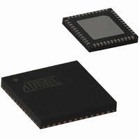
ATA5428-PLQW Atmel, ATA5428-PLQW Datasheet - Page 24

ATA5428-PLQW
Manufacturer Part Number
ATA5428-PLQW
Description
IC TXRX WIDEBND 433/868MHZ 48QFN
Manufacturer
Atmel
Specifications of ATA5428-PLQW
Frequency
433MHz, 868MHz
Data Rate - Maximum
20kbps
Modulation Or Protocol
ASK, FSK
Applications
Alarm and Security Systems, RKE
Power - Output
10dBm
Sensitivity
-112.5dBm
Voltage - Supply
2.4 V ~ 3.6 V or 4.4 V ~ 6.6 V
Current - Receiving
10.5mA
Current - Transmitting
10mA
Data Interface
PCB, Surface Mount
Antenna Connector
PCB, Surface Mount
Operating Temperature
-40°C ~ 85°C
Package / Case
48-VQFN Exposed Pad, 48-HVQFN, 48-SQFN, 48-DHVQFN
Operating Temperature (min)
-40C
Operating Temperature (max)
85C
Operating Temperature Classification
Industrial
Product Depth (mm)
7mm
Product Height (mm)
0.9mm
Product Length (mm)
7mm
Lead Free Status / RoHS Status
Lead free / RoHS Compliant
Memory Size
-
Lead Free Status / Rohs Status
Compliant
Other names
ATA5428-PLQHCT
ATA5428-PLQHCT
ATA5428-PLQWCT
ATA5428-PLQHCT
ATA5428-PLQWCT
Available stocks
Company
Part Number
Manufacturer
Quantity
Price
Company:
Part Number:
ATA5428-PLQW
Manufacturer:
LITELINK
Quantity:
106
Part Number:
ATA5428-PLQW
Manufacturer:
ATMEL/爱特梅尔
Quantity:
20 000
3.15
3.16
24
Matching Network in TX Mode
Matching Network in RX Mode
ATA5423/ATA5425/ATA5428/ATA5429
In TX mode the 20 mm long and 0.4 mm wide transmission line which is much shorter than /4 is
approximately switched in parallel to the capacitor C
C
antenna with pin RF_OUT, L
as discussed later). The transmission line can be approximated with a 16 nH inductor in series
with a 1.5 resistor, the closed switch can be approximated according to
with the series connection of 1.6 nH and 5 in this mode. To have a parallel resonant high
impedance circuit with little RF power going into it looking from the loop antenna into the trans-
mission line a capacitor of about 7.6 pF to GND is needed at the beginning of the transmission
line (this capacitor is later absorbed into C
tion). To keep the 50 impedance in RX mode at the end of this transmission line, C
be about 7.6 pF. This reduces the TX power by about 0.5 dB at 433.92 MHz compared to the
case the where the LNA path is completely disconnected.
In RX mode the RF_OUT pin has a high impedance of about 7 k in parallel with 1.0 pF at
433.92 MHz as can be seen in
120 nH and Q
impedance in TX mode for the power amplifier at RF_OUT is 890
inductor L
pared to the optimum matched loop antenna without L
this mode at 433.92 MHz, approximately an inductor of 1.6 nH in series with the parallel connec-
tion of 2.5 pF and 2.0 k . Since the impedance level at pin RX_TX1 in RX mode is about 50
this only negligibly dampens the received signal (by about 0.1 dB). When matching the LNA to
the loop antenna, the transmission line and the 7.6 pF part of C
when choosing the values of C
the transmission line with the 7.6 pF capacitor connected is 50 . Since the loop antenna in RX
mode is loaded by the LNA input impedance, the loaded Q of the loop antenna is lowered by
about a factor of 2 in RX mode; hence the antenna bandwidth is higher than in TX mode.
Table 3-11.
Note that if matching to 50 , like in
Q > 70 should be used for L
dominant. The RX and TX losses will be in the range of 1.0 dB there.
8
and C
433.92 MHz
9
Frequency
2
868.3 MHz
315 MHz
345 MHz
915 MHz
has an impedance of about 50 locking from the transmission line into the loop
and the RF_OUT pin can be estimated to be 10
L2
Impedance RF_OUT Pin in RX Mode
= 25, gives about 3.7 k loss impedance at RF_OUT. Since the optimum load
2
2
, C
to minimize its contribution to RX losses that will otherwise be
11
Table
10
and L
, C
Figure 2.2 on page
3-11. This, together with the losses of the inductor L
8
1
and C
Z(RF_OUT)RX
2.8 – j 141
2.6 – j 135
so that the impedance seen from the loop antenna into
36 – j 502
33 – j 480
19 – j 366
9
which is then higher, as needed for 50 transforma-
9
connected (using a C
9
to GND. The antenna connection between
2
and RF_OUT. The switch represents, in
8, a high Q wire-wound inductor with a
log(1 + 890/3700) = 0.95 dB com-
9
have to be taken into account
the loss associated with the
9
without the added 7.6 pF
Table 3-10 on page 23
7 k //1.0 pF
7 k //1.0 pF
7 k //1.0 pF
7 k //1.3 pF
7 k //1.3 pF
R
P
//C
4841D–WIRE–10/07
P
7
also has to
2
with


