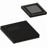
ATA5428-PLQW Atmel, ATA5428-PLQW Datasheet - Page 91

ATA5428-PLQW
Manufacturer Part Number
ATA5428-PLQW
Description
IC TXRX WIDEBND 433/868MHZ 48QFN
Manufacturer
Atmel
Specifications of ATA5428-PLQW
Frequency
433MHz, 868MHz
Data Rate - Maximum
20kbps
Modulation Or Protocol
ASK, FSK
Applications
Alarm and Security Systems, RKE
Power - Output
10dBm
Sensitivity
-112.5dBm
Voltage - Supply
2.4 V ~ 3.6 V or 4.4 V ~ 6.6 V
Current - Receiving
10.5mA
Current - Transmitting
10mA
Data Interface
PCB, Surface Mount
Antenna Connector
PCB, Surface Mount
Operating Temperature
-40°C ~ 85°C
Package / Case
48-VQFN Exposed Pad, 48-HVQFN, 48-SQFN, 48-DHVQFN
Operating Temperature (min)
-40C
Operating Temperature (max)
85C
Operating Temperature Classification
Industrial
Product Depth (mm)
7mm
Product Height (mm)
0.9mm
Product Length (mm)
7mm
Lead Free Status / RoHS Status
Lead free / RoHS Compliant
Memory Size
-
Lead Free Status / Rohs Status
Compliant
Other names
ATA5428-PLQHCT
ATA5428-PLQHCT
ATA5428-PLQWCT
ATA5428-PLQHCT
ATA5428-PLQWCT
Available stocks
Company
Part Number
Manufacturer
Quantity
Price
Company:
Part Number:
ATA5428-PLQW
Manufacturer:
LITELINK
Quantity:
106
Part Number:
ATA5428-PLQW
Manufacturer:
ATMEL/爱特梅尔
Quantity:
20 000
16. Digital Timing Characteristics
All parameters refer to GND and are valid for T
application (6V)) and V
4841D–WIRE–10/07
*) Type means: A = 100% tested, B = 100% correlation tested, C = Characterized on samples, D = Design parameter
12.1
12.2
13.1
13.2
13.3
13.4
13.5
No.
12
13
Parameters
Basic Clock Cycle of the Digital Circuitry
Basic clock cycle
Extended basic clock
cycle
RX Mode/RX Polling Mode
Sleep time
Start
Start
processing
Time for bit check
Bit
-
rate range
-
-
up PLL RX mode from IDLE mode
up signal
VS2
= 5.0V (Base
Test Conditions
XLIM = 0
BR_Range_0
BR_Range_1
BR_Range_2
BR_Range_3
XLIM = 1
BR_Range_0
BR_Range_1
BR_Range_2
BR_Range_3
Sleep and XSleep are
defined in control
register 4
BR_Range_0
BR_Range_1
BR_Range_2
BR_Range_3
Average time during
polling. No RF signal
applied.
f
Signal data rate
Manchester
(Lim_min and Lim_max
up to ±50% of t
Figure 9-4 on page
Bit
input signal f
N
N
N
N
BR_Range =
BR_Range0
BR_Range1
BR_Range2
BR_Range3
Signal
Bit-check
Bit-check
Bit-check
Bit-check
-
check time for a valid
-
= 1/(2
station Application(5V)) unless otherwise specified.
= 0
= 3
= 6
= 9
amb
Signal
t
ee
= 25°C. V
ee
)
, see
56)
ATA5423/ATA5425/ATA5428/ATA5429
VS1
Pin
= V
S2
= 3.0V (1 Li battery application (3V)), V
T
Startup_Sig_Proc
BR_Range
T
T
Symbol
Startup_PLL
T
T
T
Bit_check
XDCLK
DCLK
Sleep
Sleep
X
1024
16/f
3/f
6/f
9/f
T
Min.
Sleep
882
498
306
210
T
T
T
1.0
2.0
4.0
8.0
DCLK
16
Signal
Signal
Signal
8
4
2
1
8
4
2
DCLK
DCLK
DCLK
XTO
798.5
1/f
T
Typ.
DCLK
Signal
3.5/f
6.5/f
9.5/f
Sleep
798.5
X
1024
16/f
T
T
Max.
Sleep
VS2
10.0
20.0
882
498
306
210
T
T
T
2.5
5.0
DCLK
DCLK
16
8
4
2
1
8
4
2
DCLK
DCLK
DCLK
Signal
Signal
Signal
XTO
= 6.0V (2 Li battery
Kbit/s
Unit
ms
ms
µs
µs
µs
Type*
C
A
A
A
A
A
A
91


