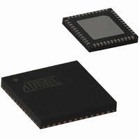
ATA5428-PLQW Atmel, ATA5428-PLQW Datasheet - Page 49

ATA5428-PLQW
Manufacturer Part Number
ATA5428-PLQW
Description
IC TXRX WIDEBND 433/868MHZ 48QFN
Manufacturer
Atmel
Specifications of ATA5428-PLQW
Frequency
433MHz, 868MHz
Data Rate - Maximum
20kbps
Modulation Or Protocol
ASK, FSK
Applications
Alarm and Security Systems, RKE
Power - Output
10dBm
Sensitivity
-112.5dBm
Voltage - Supply
2.4 V ~ 3.6 V or 4.4 V ~ 6.6 V
Current - Receiving
10.5mA
Current - Transmitting
10mA
Data Interface
PCB, Surface Mount
Antenna Connector
PCB, Surface Mount
Operating Temperature
-40°C ~ 85°C
Package / Case
48-VQFN Exposed Pad, 48-HVQFN, 48-SQFN, 48-DHVQFN
Operating Temperature (min)
-40C
Operating Temperature (max)
85C
Operating Temperature Classification
Industrial
Product Depth (mm)
7mm
Product Height (mm)
0.9mm
Product Length (mm)
7mm
Lead Free Status / RoHS Status
Lead free / RoHS Compliant
Memory Size
-
Lead Free Status / Rohs Status
Compliant
Other names
ATA5428-PLQHCT
ATA5428-PLQHCT
ATA5428-PLQWCT
ATA5428-PLQHCT
ATA5428-PLQWCT
Available stocks
Company
Part Number
Manufacturer
Quantity
Price
Company:
Part Number:
ATA5428-PLQW
Manufacturer:
LITELINK
Quantity:
106
Part Number:
ATA5428-PLQW
Manufacturer:
ATMEL/爱特梅尔
Quantity:
20 000
8. Transceiver Configuration
8.1
Figure 8-1.
8.2
Figure 8-2.
8.3
Figure 8-3.
4841D–WIRE–10/07
Command: Read TX/RX Data Buffer
Command: Write TX/RX Data Buffer
Command: Read Control/Status Register
SDO_TMDO
SDO_TMDO
SDO_TMDO
SDI_TMDI
SDI_TMDI
SDI_TMDI
Read TX/RX Data Buffer
Write TX/RX Data Buffer
Read Control/Status Register
SCK
SCK
SCK
CS
CS
CS
Command: Read TX/RX Data Buffer
Command: Write TX/RX Data Buffer
No. Bytes in the TX/RX Data Buffer
No. Bytes in the TX/RX Data Buffer
No. Bytes in the TX/RX Data Buffer
MSB
MSB
MSB
Command: Read C/S Register X
The configuration of the transceiver takes place via a 4-wire serial interface (CS, SCK,
SDI_TMDI, SDO_TMDO) and is organized in 8-bit units. The configuration is initiated with an
8-bit command. While shifting the command into pin SDI_TMDI, the number of bytes in the
TX/RX data buffer are available on pin SDO_TMDO. The read and write commands are followed
by one or more 8-bit data units. Each 8-bit data transmission begins with the MSB. The serial
interface is in the reset state if the level on pin CS = Low.
During a RX operation, the user can read the received bytes in the TX/RX data buffer
successively.
During a TX operation the user can write the bytes in the TX/RX data buffer successively. An
echo of the command and the TX data bytes are provided for the microcontroller on pin
SDO_TMDO.
The control and status registers can be read individually or successively.
LSB
LSB
LSB
ATA5423/ATA5425/ATA5428/ATA5429
MSB
MSB
MSB
Command: Read C/S Register Y
Write TX/RX Data Buffer
Data C/S Register X
RX Data Byte 1
TX Data Byte 1
X
LSB
LSB
LSB
MSB
MSB
MSB
Command: Read C/S Register Z
Data C/S Register Y
RX Data Byte 1
TX Data Byte 2
TX Data Byte 1
X
LSB
LSB
LSB
49


