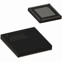
ATA5428-PLQW Atmel, ATA5428-PLQW Datasheet - Page 31

ATA5428-PLQW
Manufacturer Part Number
ATA5428-PLQW
Description
IC TXRX WIDEBND 433/868MHZ 48QFN
Manufacturer
Atmel
Specifications of ATA5428-PLQW
Frequency
433MHz, 868MHz
Data Rate - Maximum
20kbps
Modulation Or Protocol
ASK, FSK
Applications
Alarm and Security Systems, RKE
Power - Output
10dBm
Sensitivity
-112.5dBm
Voltage - Supply
2.4 V ~ 3.6 V or 4.4 V ~ 6.6 V
Current - Receiving
10.5mA
Current - Transmitting
10mA
Data Interface
PCB, Surface Mount
Antenna Connector
PCB, Surface Mount
Operating Temperature
-40°C ~ 85°C
Package / Case
48-VQFN Exposed Pad, 48-HVQFN, 48-SQFN, 48-DHVQFN
Operating Temperature (min)
-40C
Operating Temperature (max)
85C
Operating Temperature Classification
Industrial
Product Depth (mm)
7mm
Product Height (mm)
0.9mm
Product Length (mm)
7mm
Lead Free Status / RoHS Status
Lead free / RoHS Compliant
Memory Size
-
Lead Free Status / Rohs Status
Compliant
Other names
ATA5428-PLQHCT
ATA5428-PLQHCT
ATA5428-PLQWCT
ATA5428-PLQHCT
ATA5428-PLQWCT
Available stocks
Company
Part Number
Manufacturer
Quantity
Price
Company:
Part Number:
ATA5428-PLQW
Manufacturer:
LITELINK
Quantity:
106
Part Number:
ATA5428-PLQW
Manufacturer:
ATMEL/爱特梅尔
Quantity:
20 000
4841D–WIRE–10/07
AVCC is the internal operation voltage of the RF transceiver and is fed by VS1 via the switch
SW_AVCC. AVCC must be blocked with a 68 nF capacitor (see
on page 8
DVCC is the internal operation voltage of the digital control logic and is fed by VS1 or VSOUT
via the switch SW_DVCC. DVCC must be blocked on pin DVCC with 68 nF (see
page
Pin VSOUT is a power supply output voltage for external devices (for example, microcontrollers)
and is fed by VS1 via the switch SW_VSOUT, or by the auxiliary voltage supply VAUX via
V_REG2. The voltage regulator V_REG2 regulates VSOUT to typically 3.25V. If the voltage reg-
ulator is active, a blocking capacitor of 2.2 µF has to be connected to VSOUT. VSOUT can be
switched off by the VSOUT_EN bit in control register 3 and is then reactivated by conditions
found in
Pin N_RESET is set to low if the voltage V
can be used as a reset signal for a connected microcontroller (see
Figure 5-4 on page
Pin PWR_ON is an input to switch on the transceiver (active high).
Pin T1 to T5 are inputs for push buttons and can also be used to switch on the transceiver
(active low).
For current consumption reasons it is recommended to set T1 to T5 to GND, or PWR_ON to
VCC only temporarily. Otherwise, an additional current flows because of a 50 k pull-up resistor.
There are two voltage monitors generating the following signals (see
• DVCC_OK if DVCC > 1.5V typically
• VSOUT_OK if VSOUT > V
• Low_Batt if VSOUT < V
7,
Figure 2.2 on page 8
Figure 5-2 on page
and
Figure 2-3 on page
35).
ATA5423/ATA5425/ATA5428/ATA5429
Thres2
32.
and
Thres1
(2.38V typically)
Figure 2-3 on page
9).
(2.3V typically)
VSOUT
at pin VSOUT drops below 2.3V (typically) and
9).
Figure 2-1 on page
Figure 5-3 on page 34
Figure 5-1 on page
Figure 2-1 on
7,
Figure 2.2
30):
and
31


